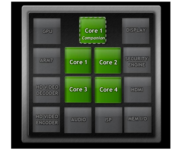
NVIDIA definitively unveiled its Tegra 3 ARM Cortex-A9-based SoC yesterday, following up on the initial disclosure at February's Mobile World Congress show (when it was known by its "Kal-El" project code name) and a subsequent release (PDF) of two architectural white papers (PDF) in late September. Those of you who have already read my technical article in last month's BDTI InsideDSP newsletter already know the bulk of the information that NVIDIA (re-)shared in last week's media briefings leading up to last night's release. The chip is advertised as a quad-core design, but it's actually a five-core topology. Here's the summary (click on the above link to my InsideDSP writeup for the rest of the story):
According to NVIDIA's documentation, the company's foundry partner offers two versions of its 40 nm process. One, referred to as "LP" (low power), uses low-leakage but slow (~500 MHz max switching speed) transistors. The other, "G" (general purpose), is capable of GHz-plus speeds but is leaky, therefore consuming more power. And even more interesting, according to NVIDIA, LP and G transistors can be combined on a single die. In reality, after subtracting out marketing hype, what NVIDIA may be describing is a single process which the company uses to selectively implement low- or high-threshold transistors for a given circuit block.
For Kal-El, NVIDIA fabricates the IC foundation, including the newly revealed fifth Cortex-A9 core, using low-power transistors, relying on high-performance transistors for the four primary Cortex-A9 cores (which are individually power-gateable this time around). In minimal workload situations, such as when a tablet is in standby mode, Kal-El turns off power to all four high performance Cortex-A9 cores, leveraging only the low-power core. Above a certain threshold, and within 2 msec, an on-chip scheduler switches over to one or multiple high-performance cores, turning off the low-power core in the process. And all of this core juggling occurs without need for operating system intervention or even awareness.

Additional details revealed this month include the following tidbits:
- The peak single-core clock speed, for the primary cores, is 1.4 GHz. When more than one primary core is operating, the peak per-core clock speed is 1.3 GHz
- The first tablet computer based on the Tegra 3 to enter volume production will be the Android-based ASUS Transformer Prime, which will be available for sale beginning some time next month for $499, and
- Rampant rumor pegs HTC's Edge as the first Tegra 3-based cellular handset
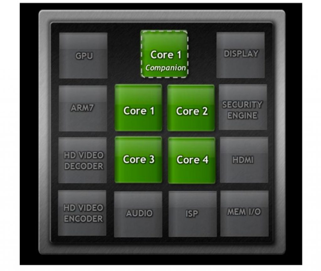
Today, however, I'd like to focus on something other that the SoC's unique multi-core arrangement. Note in the above diagram that the Tegra 3 also offers dedicated-function high-definition video encode and decode blocks, along with an ISP (Image Signal Processor) claimed twice as robust as the one in Tegra 2. Now, check out the video at the top of this writeup. What it shows is that even when decoding and displaying high-resolution still images and video frames, the Tegra 3's primary four cores are completely shut off (i.e. power-gated), and the SoC is only using only a fraction of the low-power companion core.
Presumably, although not shown in the above clip, the chip's video encode function block is equally power-efficient, as is the ISP when encoding and otherwise processing still images. The bottom line: Tegra 3 will not only deliver robust embedded vision processing capabilities, it will do so in a very battery-friendly manner. For more Tegra 3 coverage, click on the following links:


