This article was originally published at John Day's Automotive Electronics News. It is reprinted here with the permission of JHDay Communications.
By Bob Siller
Senior Strategic Marketing Manager, Automotive
Altera
In the race to develop reliable and cost-effective advanced driver assistance systems (ADAS), designers are presented with challenges to integrate functionality, develop scalable platforms and design systems that are robust enough to work in various operating conditions.
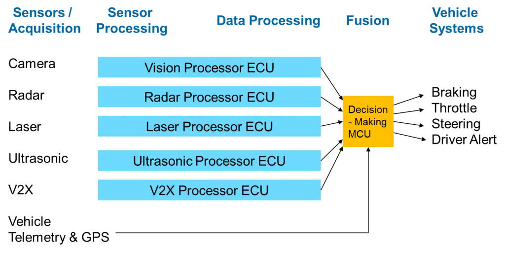
Traditional approaches to add discrete electronic control units (ECUs) for each ADAS function, like lane departure warning and forward collision warning, are not scalable and simple microcontrollers (MCUs) do not have the processing horsepower to process the various sensor inputs from multiple radars, cameras, laser scanners, ultrasonic sensors, on-board telemetry and vehicle-to-vehicle or vehicle-to-infrastructure (V2X) communications.
In this article, we will look at the various trends impacting system-level design for ADAS systems and how a new approach is necessary in order to deliver these systems into production applications.

The automotive industry is investing significant resources to develop and commercialize ADAS technology. The majority of the systems leverage multiple cameras and radars whose data is processed by sophisticated algorithms in order to become the eyes of your vehicle.
CMOS image sensors embedded in the camera modules offer megapixel resolution and new features such as high dynamic range (HDR) to improve image quality in situations with high contrast, such as driving towards a setting sun or into a dark tunnel on a bright day.
HDR image sensors typically employ a method to capture multiple exposures per frame causing an even greater increase in data bandwidth. For example, in a single HDR image sensor the video data bandwidth can approach >1Gbit per second at 720p resolution, with 20 bits per pixel and 60 frames per second. This represents a 1000 times increase of the traditional CAN network, which transmits data at 1Mbit per second and requires a high-performance data processor with more capabilities than what has been traditionally used inside a vehicle.
With increasing bandwidth requirements, automotive radar technology is trending towards transitioning from 24GHz to 79GHz frequencies. In addition, the algorithms used to process video and radar data combined with other data sources such as V2X communications, lasers scanners, on-board telemetry and ultrasonic sensors, are evolving quickly, making it difficult for automotive suppliers to determine a fixed high-performance architecture that is scalable across multiple OEM requirements.

Automotive suppliers face significant challenges to develop a base computing platform that can be quickly modified and scaled to meet the cost and performance targets in entry level and high-end luxury vehicles around the world.
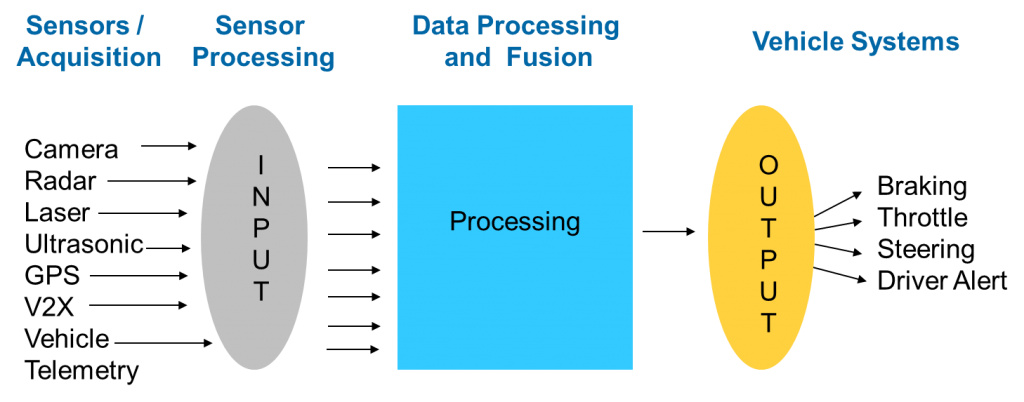
Traditionally an ASSP is selected which has fixed input and output, and processing capabilities. This approach may be sufficient for adding a specific ADAS feature in a particular vehicle model. However if suppliers want to support a wide range of vehicle models with a single hardware architecture, they will have to design for the full set of ADAS features and scale back the feature offerings on the low end vehicles. Since suppliers are using the same hardware they will have to carry extra cost for the features that will not be used in the low-end vehicles, making it difficult to be cost effective.
Another challenge with an ASSP is that it has a fixed computing architecture, which provides a set amount of resources to process sensor data. Often, the entire ASSP is consumed performing one specific algorithm, but in applications requiring multiple algorithms the processing functions need to be run in parallel.
In order to handle the increased performance requirement, either the image resolution needs to be decreased, the frame rate reduced or multiple devices need to be used. Therefore ability to add new algorithms to offer more features is also limited by a fixed computing architecture.
FPGAs present an intriguing alternative to ADAS system design compared to fixed-function devices.
FPGAs allow designers to customize the functionality and quickly change the I/O structures and hardware and data pipeline to be optimized for a particular algorithm.
For example, you can implement an FFT accelerator used for automotive radar that supports one, two or three dimensions within the same device by simply reprogramming the FPGA logic.
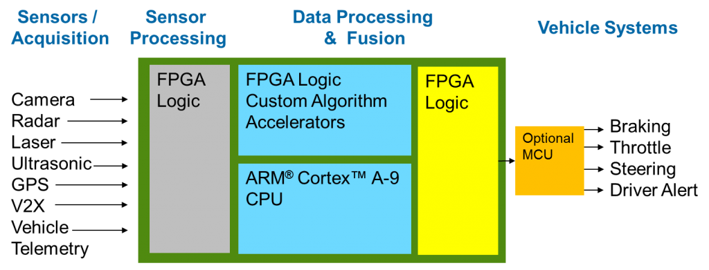
FPGAs also offer the unique capability to differentiate in both hardware and software. Altera Cyclone® V SoCs, for example, feature a dual-core ARM Cortex™-A9 processor, which operates up to 700MHz at automotive temperature ranges, up to 110K logic elements (~1.3M ASIC gates), DSP blocks and embedded memory which can provide an ideal platform for ADAS applications.
FPGAs also allow designers to create custom I/O interfaces, accelerate pixel or line-based data processing with FPGA logic, and do frame-based processing with the embedded CPU cores.
Programmable logic solutions allow designers to create a base platform with the minimum feature set and migrate to a pin-compatible, higher density device to scale up and include more processing capabilities.
With FPGAs, designers can create custom parallel processing hardware circuits to implement multiple new algorithms and reprogram the device in-system to fix bugs and add new features.

The ADAS market is rapidly evolving and so are the algorithms that power these complex life-saving systems.
Automotive OEMs need to deploy advanced ADAS technologies in their next-generation vehicle models in order to achieve five-star safety ratings as mandated by organizations such as New Car Assessment Program (NCAP).
In order to process multiple algorithms simultaneously, develop a scalable architecture, and get to market on time, ADAS system designers are increasingly turning to FPGAs and SoCs to solve their challenging problems.
The architecture of SoC FPGAs is ideally suited for vision processing applications that require both fine grained parallelism and high-level processing.
As the industry moves closer to achieving fully autonomous navigation for driverless cars, highly integrated programmable logic solutions will be increasingly adopted in vision-based applications as performance, flexibility and scalability align with the requirements for ADAS design.


