A version of this article was originally published at EE Times' Embedded.com Design Line. It is reprinted here with the permission of EE Times.
As interest grows in taking better photographs and videos and extracting knowledge from those images, innovative semiconductor architectures are emerging to provide powerful, low-power vision capabilities
By Michael McDonald
President, Skylane Technology Consulting
Consultant, Embedded Vision Alliance
The previous article in this series addressed the rapid growth in photography and computer vision – the ability to extract information from an image – and examined how computational solutions are addressing limitations in emerging camera sensors and optics. In addition to creating better photographs under increasingly difficult conditions, these same solutions are also enabling new user interfaces and experiences, creating amazing pictures that were previously impossible, and extracting information from the images to enable better management of the many photographs we are taking.
These promising new features are being added despite some major challenges. The sensor pixel size is rapidly approaching the wavelength of light, leaving limited opportunity to reduce costs by further shrinking pixels, the fundamental building block of the image sensor. In addition, the increasing performance requirements of video and vision provide challenges for mobile phones and embedded solutions that are also being called upon to run more and more applications. This article looks at some of the emerging silicon architectures – in the form of optimized and innovative processors and sensors – that are enabling these advanced features.
Quantifying the Challenge
Computer vision is a very rich source for extracting information. At the same time, it is also very complex to extract relevant information from that medium. The very powerful human brain, some neuroscientists have estimated, uses over 60% of its capacity for vision processing. There are numerous elements that contribute to vision's complexity, including the volume of data, the image pre-processing and cleanup of that data, image analysis, and resulting decision-making.
The sheer amount of data acquired in each still image and video stream is significant. Within the next two years, the outward facing cell phone camera will collect on average over 12 million pixels per image, according to industry experts (Figure 1). Many of these cameras also capture video at a rate of 15 frames per second at 12 million pixels per frame, or 30 frames per second at high definition resolutions (approximately 2.1 million pixels per frame), meaning that these cameras are generating nearly 200 million pixels per second. Emerging mobile phones will soon have the ability to capture 4k UHD (“Ultra High Definition”) video, which is over 8 million pixels per frame at 30 frames – or more! – per second or at least 240 million pixels per second. Interest in higher frame rates to capture rapid movements and generate slow-motion video clips will almost certainly increase this data rate even further.
Figure 1. Nearly half of all cell phones manufactured in 2014 are forecasted have camera sensors that are at least 8 Mpixels in resolution (courtesy OmniVision Technologies).
As these pixel values are collected, a fixed-pipeline ISP (image signal processor), either located within the image sensor or alongside it, performs image processing that is largely tied to resolving image quality issues related to the sensor and lens. A Bayer filter-pattern sensor's output data, for example, is interpolated in order to generate a full RGB data set for each pixel. The ISP also handles initial color and brightness adjustments (fine-tuned for each image sensor device), noise removal, and focus adjustment.
Once basic image processing is complete, vision processing algorithms then extract data from the image in order to perform functions such as computational photography, object tracking, facial recognition, depth processing, and augmented reality. As the functional requirements vary widely, so to will their algorithms and resulting computational load. Even a relatively simple algorithm could involve over a hundred calculations per pixel; at nearly 200 million pixels coming through the system each second, that is over 20 billion operations per second.
While powerful desktop and notebook processors operating at multi-gigahertz speeds can shoulder such a computing load, mobile phone processors are challenged to meet these vision performance requirements due to their slower clock speeds. In addition, many processor architectures frequently shuttle data in and out of cache and external memory; at the data rates required of video, this interface is a performance bottleneck and consumes significant power. In order to address these limitations, mobile processor architectures are taking advantage of acceleration engines and adding new engines specifically optimized for vision. At the same time, algorithm developers are optimizing and re-writing algorithms to run on these new engines.
New Vision Processing Architectures
New vision acceleration engines are coming in the form of GPUs, DSPs, and specialized vision processors that are capable of significantly higher levels of parallel processing. These are often SIMD (single instruction multiple data) architectures that leverage the fact that many vision algorithms perform the same functions on groups of pixels. Rather than performing the function serially on each pixel, such architectures process them in parallel, which reduces clock speed and dynamic power consumption (Figure 2). Additionally, these architectures are fine-tuned to minimize external memory accesses, enabling them to alleviate this performance bottleneck, achieve lower power consumption, and potentially lower the price of the chip package via reduced memory bus size requirements.
Figure 2. In a SIMD architecture, a single instruction is capable of working on multiple pieces of data in parallel, while a typical CPU handles data operations serially.
The increasing importance of the GPU core is reflected in its increasing percentage of the overall silicon area of a mobile application processor. Chipworks’ examination of Apple’s latest "A7" SoC, for example, reveals that a larger portion of the chip is dedicated to the GPU than to the CPU (Figure 3). Similarly, in TechInsights' examination of Samsung’s Exynos Octa mobile processor, the GPU core was larger than the combination of the quad core ARM Cortex-A15 CPU and its surrounding L2 cache memory (Figure 4). While GPUs arguably exist to support the robust gaming and other graphics capabilities of today's mobile devices, these same cores are emerging as powerful engines for computational photography and other vision applications.
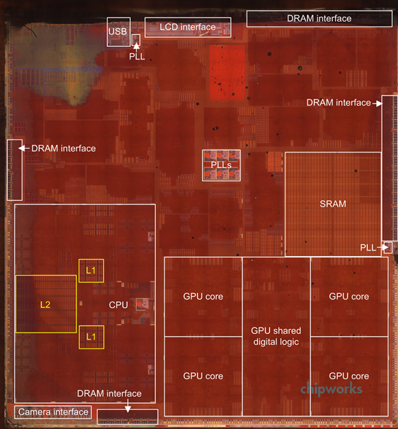
Figure 3. The GPU core and associated logic consume more silicon space than the CPU core in Apple's A7 SoC.
Figure 4. The GPU, ISP, camera and video logic take up nearly as much area as the ARM Cortex-A7 and Cortex-A15 CPUs and associated cache in Samsung’s Exynos Octa application processor.
As these applications become increasingly commonplace, optimized silicon blocks are increasingly emerging. These vision-optimized architectures have many efficient small processors that enable them to dissect an image and then process each of the resulting blocks in parallel. The companies creating these architectures also recognize the performance bottlenecks and increased power consumption that come with moving images in and out of memory and have developed approaches that eliminate unnecessary data movement.
NVIDIA, for example, introduced a computational photography acceleration engine called Chimera in the Tegra 4 SoC. Apple's advertising similarly claims that the A7 SoC contains a "new image sensor processor" enabling faster image capture, focus, and video frame rates. Qualcomm, aggressively pushing camera features such as HDR, face detection, augmented reality and other vision capabilities in the company's Snapdragon processors, integrates a "Hexagon" DSP core to offload some vision processing functions from the CPU and ISP. And the startup Movidius provides the vision and imaging coprocessor chip used in Google’s Project Tango as well as some other vision consumer products in development.
Companies whose business model involves licensing IP processor cores also recognize the parallel processing needs of these burgeoning vision applications and are responding. Many of ARM's CPU cores include the NEON SIMD processing "engine," which is often used for vision processing. Canadian company CogniVue provides licensable silicon IP core vision processor products for the automotive safety space. Core providers such as Apical, Cadence (formerly Tensilica), CEVA, Imagination Technologies, and videantis all now offer optimized cores for embedded vision that enable heavy vision processing while still fitting within the tight power budgets demanded by mobile system designs.
Modern SoC architectures typically combine GPUs and SIMD processors with traditional CPUs to create powerful vision processing platforms. Such hybrid architectures typically use more specialized cores (such as GPUs and vision coprocessors) for parallel processing of video to extract relevant objects and then use the CPU for identifying and ascertaining the meaning of those objects, making complex decisions, and acting on those decisions. The Amazon Firefly shopping application is a good conceptual (actual implementation unknown) example of how image recognition could take advantage of parallel processing engines in a GPU or SIMD architecture, while the actual shopping process may be best suited for a traditional CPU. This partitioning of the total vision task into core elements of video/vision processing and higher-level cognitive decisions helps transform a compute- and power- intensive problem into a more economical and efficient lower-power solution.
New Image Sensor Approaches
The rate of image sensor pixel size reduction is arguably slowing as the pixel size approaches the wavelength of visible light. What is not slowing down, however, are sensor technology innovations for vision. For example, emerging image sensors are moving beyond Bayer filter patterns and incorporating clear pixels that enable better image capture in low light conditions (Figure 5). This improved low-light capability comes at a price, however: the initially captured color information is less precise. Specifically, the green filters that dominate Bayer arrays, and whose portion of the visible spectrum the human eye is particularly sensitive to, are absent in some of these leading-edge approaches. Additional computation is therefore required to resolve accurate per-pixel color detail.
Figure 5. A traditional Bayer pattern image sensor focuses its data precision on the critical green frequency spectrum band, but doesn't offer the low-light performance of emerging alternative filter schemes (courtesy Aptina Imaging).
Other image sensor architectures are being explored that augment or replace red/green/blue filters with polarized filters; this can reduce glare or improve contrast. Still other architectures are being explored that add time-of-flight pixels in addition to the red/green/blue Bayer pixels; time-of-flight pixels are used to determine the distance of an object to the camera, which is extremely useful for identifying objects and understanding their shape, size, and location, as well as to assist in focusing the camera.
Innovations are also underway to increase the frame capture rate to enable slow-motion photography and effective tracking of rapidly moving objects. This greater capture rate coupled with higher per-frame resolution is rapidly increasing the amount of data that sensors must transfer, which can decrease battery life and create noisier electrical environments that degrade image quality. To address these concerns, manufacturers are developing new bus interfaces, such as CSI-3 (the third-generation Camera Serial Interface) from the MIPI Alliance, which promises to increase data rates while simultaneously decreasing power consumption and not adversely impacting image quality.
As pixel sizes shrink, image sensor manufacturers are responding by including considerably more logic on their devices, in order to create better pictures through on-chip digital signal processing. For example, in addition to managing the challenges of the previously discussed "clear pixel" and other emerging filter array structures, image sensor suppliers are exploring techniques to adjust exposure times at finer-grained levels than an entire frame. Specifically, added sensor "intelligence" discerns when additional or decreased exposure time may be needed for groups of pixels within the frame, thereby giving each area of the picture an optimized exposure. The desired end result is an overall higher dynamic range for the image, without need for the multi-image capture and post-processing used in traditional high dynamic range implementations.
Other vision sensor architectures are being examined that won’t send the actual image, but rather will send the image's meta-data. In such an architecture, object recognition would occur on the chip and only the extracted data would be sent off the sensor. This processed data could, for example, be a compact histogram of the image. While this histogram data might have limited value for a person, it is used extensively in some vision algorithms for things like image matching. By only sending the processed image, data rates are reduced, which pays dividends of lower processor speeds, slower memory busses, and lower network data rates when image information is sent into the cloud or across a network.
Adding logic to a sensor can increase heat generation and operating noise, however, which often degrades image quality. One workaround being evaluated is to use stacked die, where the bottom die contains the high-speed digital processing elements and the top die encompasses the pixels that collect light (Figure 6). Such "stacked" technology is complementary to today's increasingly common backside illumination approach, where the sensor is inverted and light is captured by the chip's "backside". In order to enable the light to penetrate the image sensor die, the wafer is thinned prior to being diced into chips, and another wafer is attached to it to provide additional structural integrity. This additional piece of silicon can also implement logic for digital signal processing capabilities.
Figure 6. A stacked die scheme could allow for the cost-effective and otherwise attractive combination of a conventional image sensor and substantial amounts of processing logic and/or local storage memory (courtesy Sony Semiconductor).
The stacked silicon approach also offers the potential to create smaller die size and lower cost “global shutter” sensors. A global shutter image sensor collects the values for all pixels and simultaneously transfers their data at a common moment in time; the global shutter differs from a “rolling shutter” where data is serially transferred off the sensor over time, rather than all at once. While the rolling shutter is a simpler architecture and enables a smaller, low-cost sensor, it distorts rapidly moving objects (Figure 7). In vision applications where a core requirement is identifying objects, global shutter sensors are often necessary to remove or totally avoid these distortions and artifacts. Existing global shutter sensors add local memory adjacent to the image sensor to store the pixel data at a common point in time until it's ready to download. With "stacked" image sensors, local memory for global shutter sensors can be moved under the image sensor, reducing the overall die size and cost of the sensor.

Figure 7. The "rolling shutter" artifacts often found when capturing images containing fast-moving subjects using conventional CMOS image sensors are not encountered with the alternative "global shutter" approach (courtesy Aptina Imaging).
Closing Thoughts and Additional Insights
The "perfect storm" of robust vision processor and image sensor technology innovations, tremendous processor performance, and strong market interest provides an exciting environment to drive tremendous growth of computational photography and computer vision in the coming years. Numerous startups are emerging from academia, where specialized vision technology has been incubating over the last twenty-plus years, and elsewhere. With the emergence of new processing architectures, both within mobile devices as well as in the "cloud", powerful vision-processing platforms now exist. They are enabling new algorithms and applications that will drive new capabilities and new growth, in a sustaining cycle that is likely to continue for quite some time.
To learn more about computational photography, computer vision, or the many applications they enable, use the various resources provided by the Embedded Vision Alliance. The Alliance is a worldwide organization of technology developers and providers whose mission is to provide engineers with practical education, information, and insights to help them incorporate vision capabilities into new and existing products. To execute this mission, the Alliance maintains a website providing tutorial articles, videos, code downloads and a discussion forum staffed by technology experts. Registered website users can also receive the Alliance’s email newsletter, among other benefits.
In addition, the Embedded Vision Alliance offers a free online training facility for embedded vision product developers: the Embedded Vision Academy. This area of the Alliance website provides in-depth technical training and other resources to help engineers integrate visual intelligence into next-generation embedded and consumer devices. Course material in the Embedded Vision Academy spans a wide range of vision-related subjects, from basic vision algorithms to image pre-processing, image sensor interfaces, and software development techniques and tools such as OpenCV. Access is free to all through a simple registration process.
The Alliance also holds Embedded Vision Summit conferences in Silicon Valley. Embedded Vision Summits are technical educational forums for product creators interested in incorporating visual intelligence into electronic systems and software. They provide how-to presentations, inspiring keynote talks, demonstrations, and opportunities to interact with technical experts from Alliance member companies. These events are intended to:
- Inspire attendees' imaginations about the potential applications for practical computer vision technology through exciting presentations and demonstrations.
- Offer practical know-how for attendees to help them incorporate vision capabilities into their hardware and software products, and
- Provide opportunities for attendees to meet and talk with leading vision technology companies and learn about their offerings.
The most recent Embedded Vision Summit was held in May 2014, and a comprehensive archive of keynote, technical tutorial and product demonstration videos, along with presentation slide sets, is available on the Alliance website. The next Embedded Vision Summit will take place on April 30, 2015 in Santa Clara, California; please reserve a spot on your calendar and plan to attend.
Michael McDonald is President of Skylane Technology Consulting, which provides marketing and consulting services to companies and startups primarily in vision, computational photography, and ADAS markets. He has over 20 years of experience working for technology leaders including Broadcom, Marvell, LSI, and AMD. He is hands-on and has helped define everything from hardware to software, and silicon to systems. Michael has previously managed $200+M businesses, served as a general manager, managed both small and large teams, and executed numerous partnerships and acquisitions. He has a BSEE from Rice University.


