This blog post was originally published at NVIDIA’s website. It is reprinted here with the permission of NVIDIA.
This is the first post in the CUDA Refresher series, which has the goal of refreshing key concepts in CUDA, tools, and optimization for beginning or intermediate developers.
Scientific discovery and business analytics drive an insatiable demand for more computing resources. Many applications—weather forecasting, computational fluid dynamics simulations, and more recently machine learning and deep learning—need an order of magnitude more computational power than is currently available, with more complex algorithms that need more compute power to run.
The computing industry has relied on various ways to provide needed performance, such as increased transistor density, instruction-level parallelism, Dennard scaling, and so on
- Increased transistor density fueled the computing demand and allowed the doubling of chip transistor density every 18 months, as predicted by Moore’s law.
- Techniques like instruction-level parallelism also helped to boost performance but returns began to diminish starting around 2001.
- Dennard scaling also provided benefits in conjunction with Moore’s law until 2005 when voltage scaling ended.
Around 2005, the historic scaling of computing started going down and the industry needed alternatives to meet computing demands. It became evident that future performance lies with parallelism.
Other key factors were power and communication. Studies showed that power was mostly spent on communication, so more communication meant more power and limiting the amount of compute that can be put in a machine. This implies that future computing should be power-efficient and locality is preferred.
Era of GPGPU
In the 90s and 2000s, graphics hardware was designed to cater to specific needs, especially for workloads in the graphics industry. But graphics workloads demanded increasing computing power. As a result, performance increased at about ~2.4x/year as compared to what transistor doubling could have provided (~1.8x/year). Figure 1 shows the famous graphics performance trajectory by Prof. John Poulton from the University of North Carolina (UNC).
Figure 1: Graphics performance trajectory circa 2001 (Source: Prof. John Poulton, UNC)
Using the metric of triangles per second, graphics hardware was increasing performance at more than 2.4 times per year, faster than Moore’s law predicted. This was due to the massive parallelism available in the computations of computer graphics, which hardware was able to leverage. In 2001, PC graphics were already spelling the end of massive systems designed for graphics.
For the developer community, this was the motivation to tap into amazing computational horsepower from graphics hardware and accelerate scientific workloads such as medical imaging, electromagnetics, and many more.
NVIDIA graphics processing units (GPUs) were originally designed for running games and graphics workloads that were highly parallel in nature. Because of high demand for FLOPS and memory bandwidth in the gaming and graphics industry, GPUs evolved into a highly parallel, multithreaded, manycore processor with enormous computational horsepower and high memory bandwidth. This started the era of GPGPU: general purpose computing on GPUs that were originally designed to accelerate only specific workloads like gaming and graphics.
Hybrid computing model
GPUs were designed for highly parallel computations and were also referred to as throughput processors. Many scientific and AI workloads have inherent massive parallelism in their algorithms and may run very slowly on CPUs.
GPU-accelerated applications offload these time-consuming routines and functions (also called hotspots) to run on GPUs and take advantage of massive parallelism. The rest of the application still runs on the CPU. You offload compute-intensive and time-consuming portions of your code to GPUs to speed up your application without completely moving your application to GPUs. This is also called a hybrid computing model.
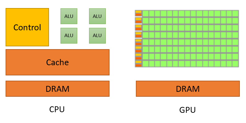
With the rise in hybrid computing, both processors co-existed but they were still fundamentally different. Figure 2 shows the fundamental difference between CPUs and GPUs.

Figure 2: GPUs devote more transistors to compute data processing.
GPUs dedicate most of their transistors for data processing while CPUs also need to reserve die area for big caches, control units, and so on. CPU processors work on the principle of minimizing latency within each thread while GPUs hide the instruction and memory latencies with computation. Figure 3 shows the difference in computation threads.
Figure 3: Low latency or high throughput.
As evident from Figure 3, CPU architectures must minimize latency within each thread. On CPUs, every thread minimizes the data access time (white bars). During a single time slice, thread gets work done as much as possible (green bar). To achieve this, CPUs require low latency, which requires large caches and complex control logic. Caches work best with only a few threads per core, as context switching between threads is expensive.
GPU architecture hides instruction and memory latency with computation. In GPUs, threads are lightweight, so a GPU can switch from stalled threads to other threads at no cost as often as every clock cycle.
As shown in Figure 3, when thread T1 stalled for data, another thread T2 started processing, and so on with T3 and T4. In the meantime, T1 eventually gets the data to process. In this way, latency is hiding by switching to other, available work. This means that GPUs need many overlapping concurrent threads to hide latency. As a result, you want to run thousands of threads on GPUs.
For more information, see the CUDA Programming Guide.
Pradeep Gupta
Director, Solutions Architecture and Engineering Team, NVIDIA


