This market research report was originally published at Yole Développement’s website. It is reprinted here with the permission of Yole Développement.
The short wave infrared (SWIR) imaging industry will drastically change. Yole Développement’s analysts highlight the rise of under-display 3D sensing applications in smartphones. But not only…
OUTLINE:
-
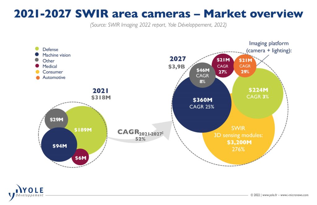
Machine vision segment will grow fast reaching US$360 million in 2027. Starting in 2023 with under-display 3D sensing applications, the consumer segment will reach more than US$3 billion four years later.
-
InGaAs is the most mature SWIR imaging technology on the market but quantum dots technology is emerging…
-
STMicroelectronics and Sony are now active in SWIR imaging industry, they might create a paradigm shift in the long term.
Lyon, France, Feb. 17th 2022 – The market research and strategy consulting company, Yole Développement (Yole), has been investigating the imaging industry for some years. Yole’s analysts have combined their expertise to deliver today a comprehensive overview of the SWIR technologies and applications with a dedicated report, titled SWIR Imaging. This new study analyzes in detail the challenges and opportunities of the SWIR industry. It provides market data on key SWIR imaging technologies and delivers a valuable understanding of the SWIR imaging value chain, infrastructure, and competitive landscape.

For Axel Clouet, Ph.D., Technology & Market Analyst, Imaging and Display at Yole: “SWIR imaging is used in defense, mainly for laser target designation. This is the largest segment by value, worth US$189 million in 2021. In machine vision, SWIR has many applications, including plastic or food sorting, solar panel inspection, and content inspection. This segment is growing faster than defense and could reach US$360 million value in 2027, up from US$94 million in 2021.”
SWIR is also advertised for automotive (ADAS applications) as it allows stable image acquisition in harsh conditions such as fog, snow, sun glare, and nighttime. The segment might start by 2024 at US$4 million, reaching US$21 million by 2027.
Finally, SWIR may be used in smartphone under-display 3D sensing since OLED displays are more transparent to SWIR wavelengths than the NIR currently used. The first commercial products could be released by 2023 and the consumer segment could generate US$3.2 billion at the module level by 2027. Eye safety regulations are less stringent in SWIR than in NIR. Besides under-display, SWIR would allow the use of more powerful illumination and generally increase range and reliability of 3D sensing solutions compared to NIR.
In 2021, the SWIR industry’s leading players were SCD, Sensors Unlimited, and Teledyne FLIR, sharing more than 50% of the 11,000 units shipped in the year. These leaders are subsidiaries of leading defense companies that started developing SWIR technology with the support of governments for strategic purposes. They constitute the legacy side of the SWIR industry.
On the other side, STMicroelectronics and Sony, two leaders in the consumer imaging industry started being active players in SWIR with new technologies including quantum dots. Their entrance might be explained by the growing demand from consumer OEM for new integration designs such as under-display 3D sensing in smartphones. If SWIR imagers reach a low price point, shipments could skyrocket to hundreds of millions within a few years. The SWIR industry could emulate the current 3D imaging industry, where STMicroelectronics and Sony share nearly 95% of the 225 million shipments (2020 data).

Acronyms:
- InGaAs: Indium Gallium Arsenide
- SWIR: Short Wave Infrared
- ADAS: Advanced Driver Assistance Systems
- OLED: Organic Light Emitting Diode
- NIR: Near Infrared
- OEM: Original Equipment Manufacturer


