-
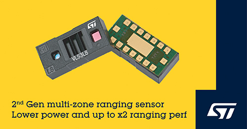
The VL53L8 direct Time-of-Flight (dToF) sensor is ideal for smartphones as well as smart speakers, human-machine interfaces, consumer LiDAR, and AR/VR/MR
-
Sensor combines new revolutionary metasurface lens technology with a more powerful and efficient laser and improved on-chip processing
09 Jun 2022 | Geneva | STMicroelectronics (NYSE: STM), a global semiconductor leader serving customers across the spectrum of electronics applications, has announced its newest FlightSense™ Time-of-Flight (ToF) ranging sensor for smart-phone camera management and augmented/virtual reality. With significant enhancements to many key components, ST’s latest ToF module offers up to double the ranging performance – up to 4m in all zones indoors — while reducing the power consumption by half compared to the previous-generation device, when operating in common conditions.
“ST’s ToF technology has enjoyed massive commercial success, now shipping in more than 200 smartphone models and 100 PC, projector, and robotic products. Now, VL53L8 FlightSense sensor takes ranging performance and power efficiency to new levels,” said Eric Aussedat, Executive Vice President and General Manager of the Imaging Sub-Group within ST’s Analog, MEMS and Sensors Group. “Our latest-generation ranging sensor is a game changer. With its innovative metasurface lens technology and power-efficient architecture, it reduces battery loading, extends camera autofocus ranging, and enhances scene-understanding features.”
Developed in partnership with Metalenz, the world’s first optical metasurface technology enables optical systems to collect more light, provide multiple functions in a single layer, and deliver new forms of sensing in smartphones and other devices, all in its compact package.
The VL53L8 is ideal for smartphones and tablets in both user-facing and world-facing applications, but also for accessories in the personal electronics segment like smart speakers and AR/VR/MR. The user-facing applications include object tracking and gesture recognition. World-facing applications include laser-autofocus, camera selection, touch-to-focus, and flash dimming – the VL53L8 will deliver even greater benefit to these features in low-light conditions. The sensor can also support indoor/outdoor detection and smart-focus bracketing, as well as consumer LiDAR, where depth mapping is required.
Technical information
The module embeds a high output 940nm VCSEL light source, a System-on-Chip sensor with an embedded VCSEL driver, the receiving array of SPADs, and a low-power 32-bit MCU core. The VL53L8 adopts a metasurface lens technology in both the transmit and receive apertures. Moreover, like the VL53L5, the new sensor delivers 16 or 64 discrete ranging zones with stable and accurate improved ranging.
The VL53L8 builds upon the innovations delivered by previous ST ToF sensors including VL53L5. The 2nd-generation ranging sensor incorporates an efficient optically diffractive metasurface lens technology, manufactured at the company’s 300mm fab in Crolles, France. In combining a new VCSEL driver 3 times more capable than the previous generation with an efficient VCSEL, the VL53L8 can, in comparable conditions, deliver twice the ranging performance of VL53L5 or reduce power consumption by 50%. It delivers this performance while maintaining the same field of view and discrete output-ranging zones (4×4 at 60 frames per second or 8×8 at 15 frames per second). For easy system integration, the sensor is housed in a single reflowable component that offers 1.2V and 1.8V I/O compatibility and significantly reduces the host processor loading over the demands of the first-generation sensor.
Like all other FlightSense ToF proximity sensors, the VL53L8 retains an IEC 60825-1 Class 1 certification and is fully eye-safe for consumer products with an advanced lens detach detection system.
The VL53L8 is entering mass production now for select customers. Please contact your ST sales office for pricing and sample requests.
About STMicroelectronics
At ST, we are 48,000 creators and makers of semiconductor technologies mastering the semiconductor supply chain with state-of-the-art manufacturing facilities. An integrated device manufacturer, we work with more than 200,000 customers and thousands of partners to design and build products, solutions, and ecosystems that address their challenges and opportunities, and the need to support a more sustainable world. Our technologies enable smarter mobility, more efficient power and energy management, and the wide-scale deployment of the Internet of Things and connectivity. ST is committed to becoming carbon neutral by 2027. Further information can be found at www.st.com.


