-
The IoT market is yet to see an “explosive growth” in TinyML. Is that due to inadequate hardware, ever-shifting software or not enough ML skills in the embedded community?
-
What’s at stake: TinyML in embedded systems can be implemented many ways, often by leveraging beefed-up MCUs, DSPs, AI accelerators and Neural Processing Units (NPUs). The lingering dilemma is how best to develop embedded systems with machine learning that could fit in the budget of TinyML.
Almost every new technology overheats its industry’s imagination, followed by an announcement flood, promising new tools, software and hardware – all of which fuels dreams of rapid market growth and big volume sales.
Then, reality.
TinyML has reached this moment.
Since TinyML’s first publication in 2019, the embedded industry has striven mightily to bring TinyML home. What they have exposed, however, is that talk is cheap, TinyML is hard.
First, embedded system engineers are not necessarily AI experts. In many cases, TinyML has proven to be the embedded system designers’ first AI project.
Assessing TinyML’s true market potential isn’t so simple, either.
TinyML is a category of Machine Learning with small-footprint models operating at low power. However, TinyML is at the mercy of the constant evolution of AI software and hardware, which can blur the definition of TinyML in the market.
Against this backdrop, Ceva launched this week what it claims as “new TinyML optimized NPUs,” dubbed Ceva-NeuPro-Nano NPUs. Ceva is confident that it has all the right technological ingredients to help system designers crack the TinyML market.
NeuPro-Nano marks Ceva’s virgin TinyML foray. The Nano’s focus is “on-device and embedded implementations of AI,” said Chad Lucien, Ceva’s vice president and general manager for sensors and audio BU.
Independent of the Nano, Ceva previously announced NeuPro-M for the Edge AI market focused on applications like generative AI and large scale NPU implementations. Both M and Nano are part of Ceva’s NeuPro NPU family.
Lucien acknowledged that the industry has yet to accept a uniform TinyML definition to which everyone adheres, since many players are using the terminology in different ways. Sticking to its own terms, Ceva says that the TinyML “typically consumes 1 watt or less, and supports 10’s of Giga-operations per seconds (GOPS) of compute.”
Ceva’s NeuPro NPU family offers an IP portfolio that scales from tens of GOPS to thousands of TOPS.

Ceva goes after a broad range of embedded AI market with different IPs. (Image: Ceva)
AI software stack
Ceva has also rolled out Ceva NeuPro Studio, an AI software stack designed to work with the NeuPro family. The stack is “built around the industry’s open standards,” ranging from TensorFlow Lite for Microcontrollers (TFLM) to microTensor Virtual Machine (µTVM), according to Lucien.
Client input taught Ceva that “one of the pain points in the AI marketplace today is the lack of common software interface across a portfolio of products,” said Lucien.
Ceva’s NeuPro Studio includes standard libraries such as the Model Zoo of trained and optimized TinyML models covering voice, vision and sensing use cases.
TinyML: Explosive growth?
ABI Research is one of the firms closely tracking the TinyML market. Its latest TinyML report is not out yet, although its release is “imminent,” according to Paul Schell, ABI’s industry analyst.
ABI, Schell acknowledged, “hasn’t [yet] witnessed explosive growth” for TinyML. But with its “adoption steadily increasing,” he remains optimistic. “The number of use cases is expanding as hardware as well as software capabilities are improving.”
Schell’s optimism for TinyML rests on several factors, including the emergence of better hardware. Also significant is improved accessibility to critical software tools.
Schell is also bullish on neural processing units (NPU), like Ceva’s NeuPro-Nano IP. He told us, “Innovations like the addition of NPUs with the ability to accelerate AI workloads will enable more demanding neural networks to run on embedded devices, especially around machine vision.” Schell elaborated: “Going from simple audio and visual detection to classification,” without NPU, would have previously needed “a significantly higher power footprint.”
He added, “Innovations in software compression techniques (e.g., quantization) for AI models also expand the number of more demanding applications that can run on embedded devices.”
ABI is also seeing progress in accessibility to MLOps and other software tools and platforms. Machine learning operations (MLOps) are a set of practices that automate and simplify machine learning workflows and deployments. These critical tools enable “models trained in the cloud to be more quickly deployed on TinyML hardware,” Schell explained. “This is accelerating time-to-value and enabling projects to breach the Proof-of-Concept stage.” Schell stressed that “offering such tools is becoming table stakes for any TinyML chip vendor.”
Why NPU for TinyML?
Given that AI – and by extension TinyML – is a moving target, semiconductor designers constantly face hard choices.
With TinyML, “one emerging area of divergence (and potentially confusion) is around ‘machine vision’ and ‘audio signal’ use cases,” noted ABI’s Schell, providing a fodder for arguing over “what was hitherto possible on MCUs vs. the more demanding workloads (such as image classification) that require an NPU or other accelerator.”
In such circumstances, many semiconductor companies approached TinyML in embedded systems via various chip solutions.
For example, many semiconductor companies “have rolled home-grown accelerators, often with hardwired NPUs,” observed Ceva’s Lucien. But when those vendors found out that their chips — designed for a specific AI task — don’t cover everything, they had to either design a new accelerator or do something different, pronto. “Multiple customers … told us that they need a new accelerator because what they’ve got reached the end of life.”
On the other hand, Lucien added, some MCUs and DSPs are “being repurposed with some special extensions to handle neural networks. Then, they add a separate NPU accelerator alongside to produce good performing solutions.”
This option might seem to solve TinyML’s performance problems. In reality, what’s left is a programming nightmare because “now that you’ve got two cores,” Lucien noted, “you must deal with the complexity of implementing software” over the two different cores. Two-core solutions have also caused headaches for system designers, including “area and cost implications, and the memory management of moving data back and forth between them.”
For Ceva, all these complications have clarified what it must offer its customers on the TinyML market. “We are focused on a fully programmable, self-sufficient single core, which is not an accelerator,” stressed Lucien. This doesn’t require “a separate CPU or DSP to operate.”
With Nano NPU, he said, “We can efficiently execute all the feature extraction together with the neural network (NN) compute in the same core. It acts as a controller, running DSP and audio code.”
Lucien explained that the architecture of its fully programmable NPU is scalable with room to add advanced machine learning processing capabilities.
Calling it “future-proof,” Ceva boasted that Nano can support most advanced ML data types and operators, including 4-bit to 32-bit integer support and native transformer computation. Nano also provides ultimate ML performance for all use cases including sparsity acceleration, acceleration of non-linear activation types, and fast quantization.
With Ceva’s Nano IP, TinyML can get integrated broadly. It can drop into an MCU, said Lucien, as the microcontroller’s NPU core. The Nano IP could also sit next to connectivity on a Bluetooth SoC for earbuds, smart speakers or sound bars. Further, Nano IP can be used in a sensor itself or installed next to a sensor.
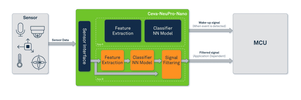
Ceva-NeuPro-Nano handles control code, NN layers and feature extraction on same processor (image: Ceva)
Competitive landscape
Although Ceva is withholding specifics on how it is benchmarking its own Nano IP against whom on the TinyML market, Ceva’s obvious rival is Arm’s Ethos. Arm was first to unveil a microNPU, a new class of ML processor designed to accelerate inference on embedded and IoT devices.
Without disclosing specifics, Ceva’s Lucien noted that NeuPro Nano brings to the TinyML market some key features that others do not.
One is the AI compression technology Ceva developed. Branded it as “Ceva-NetSqueeze,” it takes compressed model weights and feeds them into the NPU without an added step for decompression, noted Lucien. In contrast, with a dual core solution, Lucien explained that it might be necessary to decompress the weights into memory, then recompress and feed them into the NPU.
In the end, NetSqueeze enables Ceva’s NeuPro-Nano NPUs to reduce the memory footprint — a major bugaboo for AIoT processors — by 80%.
Another NeuPro Nano trick is power saving. Using sparse, non-zero weights for calculation saves power, said Lucien. But Ceva goes further, by “dynamically scaling the voltage in the frequency, based on the use case,” he added. “So, when each model may have different requirements for frequency and voltage in executing the network, you can scale the voltage in the frequency to match what’s required to run that network. And then, when you run the next network, it scales the core appropriately.”
Bottom line
Beyond fundamental issues with TinyML hardware and software, consider IoT devices’ life cycles. ABI’s Schell called the issue “one of the hang-ups” that has hampered TinyML’s growth. For existing IoT projects with life cycles five years or longer, especially in the industrial market, making TinyML a good, natural fit might be harder than one might think.
Junko Yoshida
Editor in Chief, The Ojo-Yoshida Report
This article was published by the The Ojo-Yoshida Report. For more in-depth analysis, register today and get a free two-month all-access subscription.