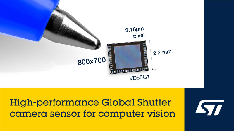
The sensor is designed for use in a range of applications, including AR/VR, personal and industrial robotics, drones, barcodes, biometrics and gestures, and embedded vision and scene recognition
Dec 7, 2023 – Geneva, Switzerland – STMicroelectronics (NYSE: STM), a global semiconductor leader serving customers across the spectrum of electronics applications, is enhancing smart computer vision with its latest global-shutter image sensor. The global-shutter sensor technology is particularly useful for capturing distortion-free images when the scene is moving or when near-infrared illumination is used.
“Our new global-shutter image sensor provides superb resolution in an extremely small die suitable for use in equipment like smart glasses and AR/VR headsets. It’s also well suited to personal and industrial robotics and smart-home devices. All these applications benefit from the sensor’s high performance, small size, ultra-low power consumption, and optimized cost,” said Alexandre Balmefrezol, Executive Vice President, Imaging Sub-Group General Manager, STMicroelectronics.
The sensor is small, measuring just 2.7mm x 2.2mm, and has a native resolution of 800 x 700 pixels. Its low power consumption means it can be used with smaller batteries, and its imaging performance is exceptional, with high contrast and superior image clarity.
The sensor also offers event-like image streaming, making it ideal for eye-tracking and other motion-estimation use cases.
This new global-shutter image sensor also comes with innovative embedded features. These features include native background removal, which reduces the post-processing workload for the host. The sensor also has an ‘always-on’ 1mW autonomous mode that allows continuous awareness even when the host is turned off, saving power. The system wakes up when a movement or scene change is detected.
In contrast to rolling-shutter sensor technology, which exposes the sensor’s image array line-by-line, global-shutter sensor technology exposes the entire image array at the same time. A global-shutter approach is advantageous in applications where the image is moving at high speed.
ST’s new VD55G1 is sampling now, with volume production slated for March 2024
ST partners offer packages and modules embedding the VD55G1 for various use cases and markets.
For more information, please go to www.st.com/en/imaging-and-photonics-solutions/vd55g1.html
Further technical information
Completing ST’s specialized sensor portfolio, the VD55G1 global-shutter sensor leverages the Company’s advanced process technologies that enable a class-leading 2.16um pixel size, high sensitivity, and low crosstalk. Together, the innovations in silicon process technology and pixel architecture minimize the sensor pixel array area on the top die, while maximizing digital-processing capabilities and features on the bottom die.
ST’s advanced pixel technology uses full Deep Trench Isolation (DTI) while optimizing performance through the combination of low Parasitic Light Sensitivity (PLS), high Quantum Efficiency (QE), and a low noise architecture.
The device is I3C-controlled for 10x faster communication, and embeds multi auto-exposure, high-framerate operation, flexible tone mapping, multiple context switches, and much more.
About STMicroelectronics
At ST, we are over 50,000 creators and makers of semiconductor technologies mastering the semiconductor supply chain with state-of-the-art manufacturing facilities. An integrated device manufacturer, we work with more than 200,000 customers and thousands of partners to design and build products, solutions, and ecosystems that address their challenges and opportunities, and the need to support a more sustainable world. Our technologies enable smarter mobility, more efficient power and energy management, and the wide-scale deployment of cloud-connected autonomous things. We are committed to achieving our goal to become carbon neutral on scope 1 and 2 and partially scope 3 by 2027. Further information can be found at www.st.com.


