Embedded vision applications deal with a lot of data; a single 1080p60 (1920×1080 pixel per frame, 60 frames per second) 24-bit color video stream requires nearly a half GByte of storage per second, along with nearly 3 Gbps of bandwidth, and 8-bit alpha (transparency) or 3-D depth data further amplifies the payload by 33% in each case. Reliably and cost-effectively storing this data, as well as rapidly transferring it between memory and other system nodes, is critical to robust system operation. As such, advanced memory technologies such as Mentor Graphics' coolSRAM-1T are valuable in embedded vision designs. This is a reprint of a Mentor Graphics-published white paper, which is also available here (1.2 MB PDF).
For more information on Mentor Graphics' Memory IP products, please visit https://www.mentor.com/products/ip/memory-ip/.
Introduction
Memory content in modern silicon chips (SoC, ASIC, etc.) is dramatically increasing as more complex functionality and software are required to run on a single monolithic chip. More complex types of IPs (intellectual properties) are also being integrated into a single chip (such as analog, CPU, DSP, OTP, SRAM, ROM, CAM, and high-performance I/Os). Chip design managers face the daunting task of making a choice for each of the IPs on a chip, which involves acquiring and digesting copious amounts of information.
This paper explores the design tradeoffs between 6T static random access memory (6T-SRAM) and Mentor Graphics’ coolSRAM-1T™ dynamic random access memory. Background information for 6T-SRAM and coolSRAM-1T technologies is covered first. The coolSRAM-1T technology is detailed in subsequent sections; followed up by a sample test report.
6-transistor Static Random access Memory (6T-SRAM)
6T-SRAM is the most widely used memory type in silicon designs today. New process nodes are typically qualified by using optimized 6T-SRAM arrays. A schematic for a 6T-SRAM static cell is shown in Figure 1.

Figure 1. 6T static random access memory (6T-SRAM) is composed of a storage latch and two access transistors that allow read and write access into the cell.
The 6T-SRAM cell consists of a storage latch (two back-to-back inverters) along with two access NMOS transistors that allow read and write access into the cell. The value stored in the cell is determined by the polarity of Q/ Q x nodes, which are opposite each other. Note that the storage nodes (Q / Q x) are actively driven at all times. The cell is read by first precharging to supply (VDD) and then floating the bitlines (bL and bLx). When wordline (WL) is driven high to VDD, the bitline connected to the side of the latch with a zero inside is pulled low while the complement bitline stays at VDD. A sense amplifier detects this differential signal and converts it to full-swing digital value. To write into the cell, the desired data value is driven onto the bitlines and the wordline is driven to VDD. The data is forced into the cell. Read/write operations on a 6T-SRAM cell are summarized in Table 1.

Table 1. Summary of 6T-SRAM operation.
The 6T-SRAM cell area is minimized by fabrication houses by extensively utilizing “pushed” design rules in the cell. Since the 6T-SRAM cells are used only in regular two-dimensional arrays, the process is optimized so that high yield is achieved with the pushed design rules. However, despite the use of pushed design rules, the 6T-SRAM cell contains six transistors and is quite a bit larger than single transistor/capacitor dynamic memory. Since 6T-SRAM also uses active drivers to maintain data, leakage power becomes a major concern in advanced process nodes. On the other hand, coolSRAM-1T uses passive storage structures that are optimized for low leakage and tend to have a lower leakage current in advanced technology nodes.
coolSRAM-1T Embedded Dynamic Random Access Memory
Dynamic random access memory (DRAM) can be a cost-effective alternative to 6T-SRAM since it occupies a smaller area. However, conventional DRAM bitcell implementations require additional process steps that add to the wafer cost and diminish or completely erase any area savings that DRAM provides.
Mentor Graphics’ coolSRAM-1T uses only the standard base CMOS process, providing design flexibility and cost savings. The interface to the memory blocks looks very much like a 6T-SRAM, providing random access every cycle (i.e., RAS/CAS page access patterns found in stand-alone DRAM architectures are not used).
The coolSRAM-1T dynamic memory cell consists of a storage capacitor and an access transistor. Because the capacitor provides a passive storage medium (there is no active drive on the storage node Vcell), minimizing the leakage currents in the cell is extremely critical to a successful dynamic memory implementation. The coolSRAM-1T is shown in Figure 2.

Figure 2. coolSRAM-1T dynamic memory cell with a storage capacitor and an access transistor. The passive nature of the cell requires extremely low leakage currents.
Typically, the cell is read by biasing the bitline (bL) at approximately half supply voltage and then floating it. The wordline (WL) is then driven to high, and the charge stored inside the cell is dumped onto the bitline. The small voltage change on the bitline is sensed by an amplifier. Since the read is destructive (the act of reading destroys the data in the cell), after being sensed, the data is written back into the cell. Writing into the dynamic memory cell is accomplished by driving the bitline to the desired data and then driving the wordline high. The dynamic memory operation is summarized in Table 2.

Table 2. Summary of dynamic memory operation.
The charge inside the cell is passively stored, so any source of leakage will slowly decrease the amount of charge originally written into the cell. A periodic refresh is therefore needed to maintain data indefinitely in a dynamic memory cell. A simple refresh can be accomplished by the system accessing a memory location. Typically, dynamic memory blocks have a refresh interface that allows a memory location to be refreshed without affecting the instance output and provides the ability to refresh more than one entry at a time.
One of the major challenges of dynamic memory design is the loss of stored charge due to leakage. Four major sources of leakage in a dynamic memory cell are demonstrated in Figure 3. The access transistor will have subthreshold leakage during idle state (depending on the bias conditions of the bitline) and especially when a “0” is written to another row in the same block. Subthreshold leakage is exponentially dependent on device threshold voltage and gate-source overdrive voltage. As the gate oxide thickness is scaled to below around 30 angstrom, the gate leakage starts to become a significant source of charge loss. Depending on the physical implementation details of the capacitor, there might be appreciable leakage through the storage capacitor. Finally, the junction of the access transistor will leak charge into the bulk. Junction leakage can be minimized by optimizing the cell layout structure and the fabrication process.

Figure 3. Four major leakage sources in a dynamic memory cell.
To minimize the cell leakage and provide a large storage capacitance in a small area, the DRAM process has diverged from the standard baseline digital CMOS process. In recent years, due to increasing requirements for large amounts of embedded memory in SOC applications, DRAM process modules have been designed to be plugged into the standard CMOS process flow. However, such process modules increase the mask and wafer costs, so there is a minimum cost barrier to utilizing DRAM on chips.
Mentor Graphics’ innovative coolSRAM-1T technology uses the standard CMOS process to implement the dynamic memory cell and can reduce the memory area by half with no additional mask or wafer costs. Mentor Graphics’ coolSRAM-1T design is also foundry or factory-independent and can be ported quickly.
The basic requirements of a robust DRAM are that it have adequate storage capacitance in a small area, very small cell leakage, and robust peripheral sense circuits. Mentor Graphics’ coolSRAM-1T utilizes process options available in the standard CMOS process to build the cell and circuits that satisfy the above requirements.
coolSRAM-1T Cell In Standard CMOS
To minimize subthreshold and junction leakage, the Mentor Graphics’ coolSRAM-1T dynamic memory cell utilizes the thick oxide or input/output (I/O) transistor option available in all advanced process nodes. Thick oxide devices have larger oxide thickness, higher threshold voltage, and deeper junction characteristics. In addition to much lower leakage levels, the thick oxide devices are also able to withstand higher gate and drain voltages, therefore enabling more charge storage in the same cell area. An important physical parameter for the cell is the amount of charge stored: Q = C V, where Q is the amount of charge stored, C is the cell capacitance, and V is the voltage in the cell. Note that the cell capacitance and cell voltage are interchangeable.
The storage capacitor can be implemented as the gate oxide capacitance of a thick oxide device. In advanced technology nodes (e.g., 65nm and below), the use of metal-to-metal capacitance as the storage medium becomes more area efficient than planar gate oxide capacitance. The interconnect conductor spacing becomes smaller with each technology generation, resulting in larger capacitance compared to the unit capacitance that can be obtained from a thick oxide gate. Figure 4 illustrates the coolSRAM-1T cell implementation.
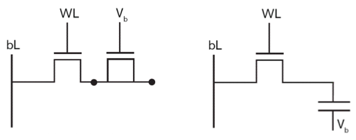
Figure 4. Mentor Graphics’ coolSRAM-1T cell implementation with thick oxide devices. The basic device characteristics for a given oxide thickness remain the same at different technology nodes. The cell capacitance is implemented with metal fringe capacitors in the most advanced process nodes.
The basic device characteristics for thick oxide devices remain the same from one technology node to the next (e.g., 50 Å, 2.5V I/O devices have the same oxide thickness and threshold voltage at 130nm and 90nm technology nodes). Since the device characteristics are the same, it is easier to port and characterize the coolSRAM-1T technology when the same oxide thickness option is used. Within the same technology node, variation in the implementation of the coolSRAM-1T technology is required for different gate oxide process options: 130nm 1.2V/2.5V process will have a different compiler than 130nm 1.2V/3.3V process.
Peripheral Circuit Implementation
The most important parts of the peripheral circuits are (1) the sense amplifier and (2) the write-back circuit that restores the charge into the cell after a destructive read. The sense amplifier is a sophisticated analog circuit that accurately senses the small signal from the cell injected onto the bitline. After the sensing phase is complete, the write-back circuit drives the bitlines full-swing to restore the charge into the cell after the destructive read. The sense amplifier must have a very high sensitivity as well as a high tolerance to noise and process variations. Appropriate steps are taken during design to guarantee excellent margins on silicon—as verified on coolSRAM-1T designs incorporated into customers’ products. To boost the signal in a given cell capacitor area, the cell array is operated at I/O voltage level. A larger voltage stored in the cell results in a larger signal for the sense amplifier and improves overall performance. The interface to the system is at the VDD (core) voltage level. A large number of patents have been filed on various aspects (cell, peripheral circuits to top level architecture) of this innovative technology.
The signals must be level-shifted from one voltage domain to another as they travel from the memory interface to the cell array. Tradeoffs for each design style must be carefully considered. Table 3 lists tradeoffs for three different approaches to implementing the coolSRAM-1T voltage domains: (1) memory array and the sense amplifier running at VDD, (2) memory array at VIO and the sense amplifier at VDD, and (3) memory array at VIO and sense amplifier at VIO. These three different approaches are represented in Figure 5.

Table 3. Comparison of different voltage-domain partitioning in Mentor Graphics’ coolSRAM-1T.
Independent of the size of a coolSRAM-1T instance, the cycle time is limited by the amount of time it takes a local bank (memory cells, sense circuits, and x-decoders) to correctly sense the signal from the cell, amplify, write back, and precharge to get ready for the next access into the block. The system clock frequency need not be limited by this local bank cycle time requirement if there is any known access pattern into the memory. For example, if a local bank can be guaranteed not to be accessed in two consecutive cycles, the system can run at twice the local bank frequency without having to introduce pipelining inside the bank itself.
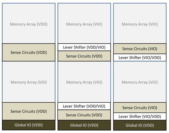
Figure 5. Architectural representation of different voltage-domain partitioning options. The represented memory is partitioned into two independent local banks. Left to right – VDD sense amp/VDD cell, VDD sense amp/VIO cell, VIO sense amp/VIO cell.
This concept of interleaving accesses into the memory is demonstrated for the case of a 2-way interleaving, shown in Figure 6. The interleaving concept is expandable to n-way interleaving if a bank is guaranteed to be accessed only once per n-cycles (and there are at least n local independent banks inside the memory instance)—with the system clock running n-times faster than the local bank.
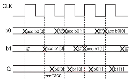
Figure 6. Example of interleaved access to two local banks (b0 and b1). Each bank is accessed in alternating cycles, and the system clock runs at twice the frequency of a local bank.
coolSRAM-1T Compilers
The Mentor Graphics coolSRAM-1T solution is integrated into the MemQuest™ Memory Compiler environment where instances can be compiled and verified (including full spice simulation characterization). Compiled instances in the 160nm 1.8V/3.3V, 130nm 1.5V/3.3V, and 110nm 1.2V/3.3V technology nodes have been incorporated into customer products and are in volume production. The memory architecture can support large instance sizes (e.g., 4Mbits or larger) as well as extreme aspect ratios. Extreme aspect ratios (e.g., height -to-width ratio of 1:20) are useful in applications such as LCD drivers where the chip height is typically limited to less than 1mm.
The compiled coolSRAM-1T memories maintain area savings over the 6T-SRAM in each technology node down to 65nm. Table 4 summarizes area savings for a typical 1Mbit instance in each technology node from 180nm to 65nm.

Table 5. Area savings of Mentor Graphics’ coolSRAM-1T over Mentor Graphics’ coolSRAM-6T™ in various standard process nodes.
If the coolSRAM-1T architecture drives the bitlines to VIO, the active power for the coolSRAM-1T will be larger than that of a similar 6T-SRAM implementation. However, in advanced technology nodes, the coolSRAM-1T instance has lower leakage, especially at high temperatures (since dynamic memory cells are optimized for low leakage with the use of thick oxide devices). Overall system power performance would have to be carefully evaluated based on the time periods that the memory is in active usage or standby. In general, coolSRAM-1T provides a better leakage performance in advanced, especially generic, process nodes.
In some designs, depending on size, the customer should consider bitcell redundancy to improve yield or retention time. Mentor Graphics’ coolSRAM-1T comes with an optional, built-in, column redundancy that is fully compatible with Mentor Graphics’ Tessent® product suite. Another consideration with memory-intensive SOC designs is for the customer to use some form of ECC. ECC should not be considered as a direct replacement for column redundancy; column redundancy is recommended for large instances even when ECC is used.
Testing
Testing procedures for Mentor Graphics’ coolSRAM-1T memory are summarized below. More information is provided to Mentor Graphics’ licensees in datasheets and test documentation. The goals of testing are (1) to identify defective parts and (2) to improve quality in the field, i.e., to identify parts that might fail a short time after being produced or fabricated. The coolSRAM-1T test flow to accomplish these goals has three major steps.
The first step in testing is to internally stress the instance at an elevated voltage, outside of the normal operating conditions. This is the voltage over-stress condition where the cell storage capacitors, bitlines, wordlines, and other signals are biased in parallel at a dc voltage for a set duration at elevated voltage and temperature levels. The memory interface provides a mode pin to automatically invoke this test condition. The intent is to aggravate internal weak defects that might become full-blown failures a short time after deployment in products.
The second step is to run the SRAM-style Built-In-Self-Test (BIST) algorithm. This algorithm checks for any defects or failing peripheral circuits by running a succession of patterns through the memory (e.g., March C+ algorithm). This testing is carried out in a tightened margin environment (high-temperature, low-voltage conditions). Additionally, proprietary interface pins allow users to further squeeze internal voltage and timing margins of the instance during BIST tests. When the instance passes the BIST tests with reduced internal margins and aggressive test conditions, it will be more likely to withstand the stress of operation and aging in the field.
Finally, the cell retention is verified under similar reduced-margin conditions as those conditions mentioned above (both voltage/temperature and internal circuit settings). The retention is verified at a longer time than what is guaranteed at a given temperature. The retention margin is sometimes implemented by margining the temperature (testing for retention at a higher temperature than maximum operation voltage specified for the part).
Testchip Shmoo Results
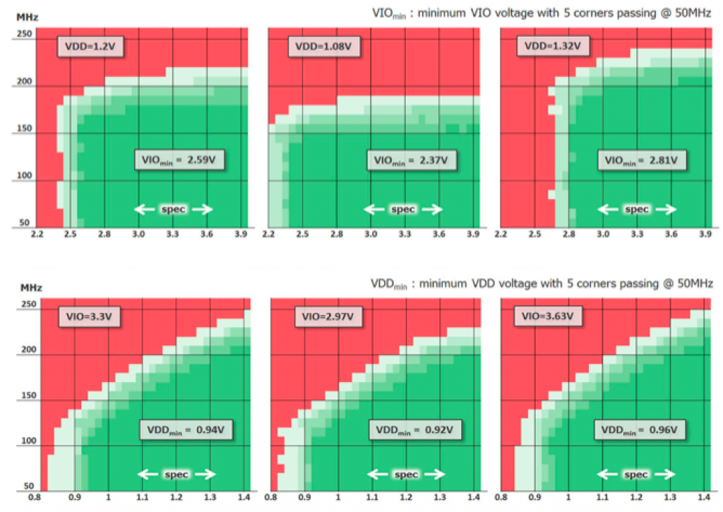
Example shmoo plots from Mentor Graphics’ 110nm test report are shown in Figure 7. Contact Mentor Graphics for full test report, or for availability of other technologies test reports. Chips are chosen from 5 process corners (TT, SS, FF, SF, FS) and must pass the BIST algorithms to qualify as a pass. The results below are shown at 25°C, but plots are also generated at hot and cold temperatures. A total of six plots are generated for each memory and temperature, as a result of the multiple supply voltages. For each plot, one power source is swept while the other power source is held constant at nominal, nominal+10%, or nominal-10%. These shmoo are healthy and show a robust operation of Mentor Graphics’ coolSRAM-1T memory.

Figure 7. Example shmoo plots at 25°C from 110nm test report. The top 3 plots sweep VIO voltage with a constant VDD supply. The bottom 3 plots sweep VDD voltage with a constant VIO supply.
Testchip Retention Results
To determine the minimum refresh frequency required for the coolSRAM-1T, retention time is measured instead of the standard 6T-SRAM retention voltage. The testing procedure for acquiring data retention time is a five step process. Direct access is first used to write a portion of the memory with a known data pattern consisting of 1’s and 0’s. Then the memory is disabled by asserting chip-enable low. Wait for a set duration. Afterward, assert chip-enable high, and read the data to confirm that there is no data loss. Increase wait time duration and repeat reading and confirming data until a failure occurs. Figure 8 shows the retention time dependency on temperature. Testing is performed on FF parts at nominal-10% VIO, which is the worst case retention corner due to the higher leakage and lower storage voltage level. The retention time results were in line with Mentor Graphics’ simulation results.
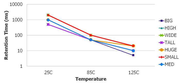
Figure 8. Example retention time vs. temperature from 110nm test report.
Cost Analysis
In a bulk CMOS design, whenever the power and speed performance targets are satisfied and over 1Mbit of memory is needed, it is more cost-effective to use Mentor Graphics’ coolSRAM-1T to replace 6T SRAM since extra mask or wafer cost are not required. In most advanced technology nodes, there has been a trend to integrate metal-insulator-metal (MIM) capacitor structures to implement dynamic memory storage capacitor. However, such additional process steps increase both mask and wafer cost. In such a scenario, the following cost analysis applies in choosing between coolSRAM-1T and MIM-based DRAM.
Although Mentor Graphics coolSRAM-1T does not require any extra mask or process steps, the resulting memory density is lower than the memory designed with MIM-based process. Therefore, there is a break even point between using Mentor Graphics solution and MIM-based solution. The break even point is given by
X ≤ (1-1/n)/(1-1/m)
Where X is the fraction of the chip that is coolSRAM-1T (e.g. X = 0.3 if 30% of the chip is occupied by coolSRAM-1T), n is the wafer cost increase factor when MIM module is added (e.g. n = 1.2 for 20% increase in wafer cost for MIM addition) and m is the size increase factor between using MIM-based solution and Mentor Graphics solution (e.g. m = 1.3 when Mentor Graphics solution is 30% larger than the corresponding MIM- based solution).
Note that this model does not include an increase in mask set costs, process development costs incurred by the factory, and the restriction of factory choice when using this MIM technology. In some cases, DRAM MIM process option may be incompatible with other process options (such as RF module). An example cost-analysis graph is included in Figure 9 with typical area and cost-factor parameters in a 65nm technology node. The Mentor Graphics’ solution is better or comparable in cost to MIM up to about 40% memory content on the chip – not considering the MIM increase in mask cost and limitation on factory choice.

Figure 9. Example retention time vs. temperature from 110nm test report.

