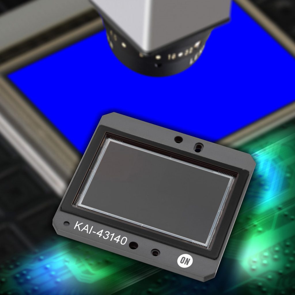
New KAI-43140 image sensor from ON Semiconductor provides fast, easy, scalable upgrade path from existing devices
PHOENIX, Ariz. – March 6, 2018 – ON Semiconductor (Nasdaq: ON), driving energy efficient innovations, is extending capabilities for critical high resolution industrial imaging with the introduction of a new 43 megapixel (MP) resolution, charge-coupled device (CCD) image sensor in the convenient 35 mm optical format. The KAI-43140 is ideal for use in applications where both very high resolution image capture and excellent image uniformity is required, such as end of line inspection of high-definition (HD) and ultra-high-definition (UHD) flat panel displays and aerial photography.
The KAI-43140 utilizes a new 4.5 µm Interline Transfer CCD (ITCCD) pixel that increases resolution by 50% compared to the prior 5.5 µm design while preserving critical imaging performance. Featuring a true electric “global” shutter, the device supports full resolution frame rates up to 4 fps through the use of flexible 1, 2, or 4 output readout architecture. The KAI-43140 shares the same package and pin definitions as the popular 29 MP KAI-29050 and KAI-29052 image sensors, allowing it to be incorporated into existing camera designs with only minor electrical changes – speeding time-to-market for adoption of the new device while retaining continuity with existing camera and lens installations.
The KAI-43140 provides very high resolution with high quality, highly uniform image capture across a wide range of exposure times, a combination that is critical for applications such as flat panel inspection, where the resolution demands of the inspection system track with the ever-increasing resolutions of displays themselves. The new device also enables surveillance and aerial photography systems to capture more detailed imagery, or capture at a higher altitude to speed acquisition time and lower costs.
“Many industrial imaging applications demand the image uniformity currently only available from CCD technology, while needing the resolution increases that require continued pixel development,” said Herb Erhardt, Vice President and General Manager, Industrial Solutions Division, Image Sensor Group at ON Semiconductor. “With the KAI-43140, camera manufacturers and end customers can continue to push the boundaries of high resolution image capture without sacrificing the image quality their applications require.”
Engineering grade versions of the KAI-43140 are now available, with production versions planned for early 3Q18. The KAI-43140 is available in a ceramic PGA package, and is offered in monochrome, Bayer Color, and Sparse Color configurations.
To help customers in the development of new camera designs incorporating the KAI-43140 and other image sensors from its portfolio, ON Semiconductor offers kits that support full evaluation including still image and video capture, region of interest (ROI) readout and pixel binning. Other custom test functions can also be configured. Customers can purchase an evaluation kit, or enquire about an on-site demonstration of the KAI-43140, by contacting their local ON Semiconductor sales representative.
Additional resources & documents:
About ON Semiconductor
ON Semiconductor (Nasdaq: ON) is driving energy efficient innovations, empowering customers to reduce global energy use. The company is a leading supplier of semiconductor-based solutions, offering a comprehensive portfolio of energy efficient, power management, analog, sensors, logic, timing, connectivity, discrete, SoC and custom devices. The company’s products help engineers solve their unique design challenges in automotive, communications, computing, consumer, industrial, medical, aerospace and defense applications. ON Semiconductor operates a responsive, reliable, world-class supply chain and quality program, a robust compliance and ethics program, and a network of manufacturing facilities, sales offices and design centers in key markets throughout North America, Europe and the Asia Pacific regions. For more information, visit http://www.onsemi.com.
- Follow @onsemi on Twitter.


