DNNs (deep neural networks) have transformed the field of computer vision, delivering superior results on functions such as recognizing objects, localizing objects within a frame, and determining which pixels belong to which object. Even problems like optical flow and stereo correspondence, which had been solved quite well with conventional techniques, are now finding even better solutions using deep learning techniques. But deep learning is also resource-intensive, as measured by its compute requirements, memory and storage demands, network latency and bandwidth needs, and other metrics. These resource requirements are particularly challenging in embedded vision designs, which often have stringent size, weight, cost, power consumption and other constraints. In this article, we review deep learning implementation options, including heterogeneous processing, network quantization, and software optimization. Sidebar articles present case studies on deep learning for ADAS applications, and for object recognition.
Traditionally, computer vision applications have relied on special-purpose algorithms that are painstakingly designed to recognize specific types of objects. Recently, however, CNNs (convolutional neural networks) and other deep learning approaches have been shown to be superior to traditional algorithms on a variety of image understanding tasks. In contrast to traditional algorithms, deep learning approaches are generalized learning algorithms trained through examples to recognize specific classes of objects.
Since deep learning is a comparatively new approach, however, the usage expertise for it in the developer community is comparatively immature versus with traditional alternatives. And much of this existing expertise is focused on resource-rich PCs versus comparatively resource-deficient embedded and other designs, as measured by factors such as:
- Image capture (along with, potentially, depth discernment) subsystem capabilities
- CPU and other processors' compute capabilities
- Local cache and chip/system memory capacities, latencies and bandwidths
- Local mass storage capacity, latency and bandwidth, and
- Network connectivity reliability, latency and bandwidth
This article provides information on techniques for developing robust deep learning-based vision processing SoCs, systems and software for resource-constrained applications. It showcases, for example, the opportunities for and benefits of leveraging available heterogeneous computing resources beyond the CPU, such as a GPU, DSP and/or specialized processor. It also discusses the tradeoffs of various cache and main memory technologies and architectures, implemented at both the chip and system levels. It highlights hardware and software design toolsets and methodologies that assist in the optimization process. And it also introduces readers to an industry alliance created to help product creators incorporate vision capabilities into their hardware and software, along with outlining the technical resources that this alliance provides (see sidebar "Additional Developer Assistance").
Defining the Problem
Why is developing a deep learning-based embedded vision design, along with adapting a deep learning model initially targeting a PC implementation, so challenging? In answering these questions, the following introductory essay from Au-Zone Technologies sets the stage for the sections that follow it.
At the core of the constrained-resources predicament is the reality that technology innovations typically originate in academic research. Both here and often with the initial profitable commercial opportunities that follow, development and implementation both typically employ a desktop- or server-class computer platform. Such systems contain a relative abundance of processing, memory, storage and connectivity resources, and they're also comparatively unhindered by the size, weight, cost, power consumption and other constraints that are conversely common in embedded design implementations. Whereas a PC developer might not think twice about standardizing on high precision floating point data and calculations, for example, an embedded developer would need to rely on low-precision fixed-point alternatives in order to balance the more challenging resource "budget."
Some specific examples of constraints and other development challenges in embedded implementations include:
- The tradeoffs between (more expensive but faster and more power efficient) SRAM and (cheaper but slower and higher power) DRAM, both at a given level in the system memory hierarchy and as subdivided (both in terms of type and capacity) among various levels.
- The increased commonality of a unified system memory approach shared by various heterogeneous processors (versus, say, a dedicated frame buffer for a GPU in a PC), and the increased resultant likelihood of contention between multiple processors for the same memory bus and end storage location resources.
- Vision processing pipelines, along with low-level drivers, that may be "tuned" for human perception, and therefore conversely may be sub-optimal for computer vision purposes.
- Software APIs, frameworks, libraries and other standards that are immature and therefore in rapid evolution.
- The oft-necessity for purpose-built development tools, custom inference engines, and the like, along with the subsequent inability to easily migrate them to other implementations.
And how do these and other factors adversely affect embedded vision development? Whether defined by available compute resources, memory and mass storage capacity and bandwidth, network connectivity characteristics, battery capacities, the thermal envelope, size, weight, bill-of-materials costs, or the combination of multiple or all of these and other factors, these constraints fundamentally define what capabilities your product is able to support and how robustly it is able to deliver those capabilities. And equally if not more importantly, they affect how long your product will spend in development, not to mention the required project budget and manpower headcount, in order to hit necessary capability targets.
Brad Scott
President, Au-Zone Technologies
Heterogeneous Processing
Computer vision and machine learning present low-power mobile and embedded systems with significant challenges. It’s important, therefore, to leverage every bit of the computing potential present in your SoC and/or system. Designing from the outset with processing efficiency in mind is key. Dual-core CPUs first came to mainstream PCs in the mid-2000s; in recent years, multi-core processors have also become common in smartphones and tablets, and even in various embedded SoCs. GPUs, whether integrated in the same die/package as the rest of the application processor or in discrete form, are also increasingly common.
Modern embedded CPUs have steadily improved in their ability to tackle some parallel tasks, as vector-based SIMD (single instruction multiple data) architecture extensions, for example, become available and are leveraged by developers. Modern embedded GPUs have conversely approached the same problem from the opposite direction, becoming more adept at some serial tasks. Together, the CPU and GPU can handle much if not all of the machine learning workload.
A key message when it comes to processor choice, in considering the spectrum of possible vision and machine learning workloads, is that a one-size solution can't possibly fit all possible use cases. Thinking heterogeneously when designing your SoC or system, leveraging a selection of processors with strengths in different areas, can reap dividends when it comes to overall efficiency. For example, many modern SoCs already come equipped with both "big" and "little" CPUs (and clusters of them), along with a GPU. The “big” CPU cores are present for moments (often short bursts) when high performance is needed, while the “little” cores are intended for sustained processing efficiency, and the GPU delivers as-required massively parallel computation ability. When used intelligently, via use of the OpenCL API and other programming techniques, you end up with a great deal of efficient processing power available to you.
The challenge, of course, is efficiently spreading your machine learning and computer vision pipeline workloads across all available computing resources in such a heterogeneous fashion. A common technique for these kinds of pipelines, when implemented on desktop or server systems, is to make many copies of large data buffers. On mobile and embedded systems, conversely, such memory copies are highly inefficient, both in terms of the time taken to perform the copies, and (crucially) in the amount of energy these sorts of operation consume. Fortunately, however, embedded and mobile SoCs typically implement a unified, global memory array, making the “zero-copy” ideal at least somewhat feasible in reality.
A remaining problem, at least historically: the CPU and GPU have separate caches, which means that transferring workloads between processors has typically required expensive (in terms of latency and/or power consumption) synchronization operations. Any potential performance gains made when moving workloads between processors can be negated in the process. These days, fortunately, designing your SoC using a modern, cache-coherent interconnect can make all the difference. Caches are kept up-to-date automatically, which means that you can more freely swap workloads between various processor types.
The inclusion of computer vision and deep learning accelerators alongside CPUs and GPUs in modern SoCs is becoming increasingly commonplace. The following essay from Synopsys discusses their potential to boost the performance, along with lowering the energy consumption, of deep learning-based vision algorithms, as well as providing various implementation suggestions.
Along with facing the usual embedded challenges of power and area consumption, a designer architecting an embedded SoC for computer vision and deep learning must also tackle some unique challenges and constraints, such as steadily increasing system complexity and the rapid pace of technology advancement. Power and area constraints therefore need to be balanced against performance and accuracy targets; the latter is very important for object detection and classification tasks, which are increasingly implemented using deep learning techniques. And memory bandwidth can also become a limiting factor that requires insight and understanding.
An embedded vision SoC, such as one based on Synopsys’ DesignWare EV6x processor family, combines both traditional computer vision processing units and newer deep learning engines (Figure 1). The EV6x includes a vision processor that combines both scalar and vector DSP resources, along with a programmable CNN engine. The scalar unit is programmed via a C/C++ compiler, while the vector unit is programmed using an OpenCL C compiler. A CNN graph, such as AlexNet, ResNet, or VGG16, is trained using Caffe, TensorFlow or another software framework, and is then mapped into the CNN engine’s hardware. The CNN engine is programmable in the sense that any graph can be mapped to its hardware.
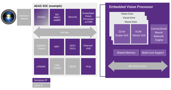
Figure 1. The various components of an embedded vision SoC can together implement a robust ADAS or other processing solution (courtesy Synopsys).
These three heterogeneous processing units deliver the best performance for a given power and area, because they are each optimized for their specific tasks. Each dedicated processing unit must be programmed, so designers need a robust set of software tools that enable mapping of embedded vision solutions across the processing units. DesignWare EV6x processors, for example, are fully programmable and supported by the MetaWare EV development toolkit, which includes software development tools based on the OpenVX, OpenCV and Open CL C embedded vision standards.
Performance, power and area are some of the constraints that need to be balanced against each other. Different projects will have different prioritization orders for these and other constraints. An automotive ADAS (advance driver assistance system) design based on a high-resolution front camera might prefer to prioritize performance, but limitations in clock speed defined by process technology (and associated cost), power consumption (and associated heat dissipation) and other parameters will constrain the SoC's maximum performance capabilities (see sidebar "Optimization at the System Level, An ADAS Case Study"). Selecting a processing solution that allows for scaling of the CNN engine can be an effective means of trading off various constraints.
Performance
Evaluating the performance of different embedded vision systems is not a straightforward process, since no benchmark standard currently exists. Comparing the number of multiply-accumulators (MACs) in different CNN engines can provide a first-order assessment, since CNN implementations require a large number of MACs. TeraMAC/s has therefore become a popular metric for specifying CNN engines. The EV6x, for example, can scale from 880 to 3,520 MACs, which at a 1,280 MHz clock frequency (under typical operating conditions and when fabricated on a 16 nm process node), delivers a performance range of 1.1 to 4.5 TMAC/s. Obscured by this metric, unfortunately, is the MACs' precision. Two different CNN engines, for example, may look similar from a TMAC/s standpoint:
880 12b MAC x 1,280 MHz = 1.1TMAC/s
1,024 8b MAC x 1,000 MHZ = 1TMAC/s
What is missing from these high-level TMAC/s performance numbers, however, is the bit resolution of the MACs in each CNN engine.
Accuracy
Bit resolution can significantly impact system accuracy, a critical metric for an application such as a front camera in an automobile. Most embedded vision CNNs exclusively use fixed-point calculations, versus floating-point calculations, since silicon cost (therefore the amount of silicon area consumed) is a key design parameter. The EV6x, for example, uses optimized 12-bit integer MACs that support 12- or eight-bit calculations. Most CNN graphs can be executed with eight-bit precision and no loss of accuracy; however, some graphs benefit from the additional resolution that a 12-bit MAC provides.
A deep graph, such as ResNet-152, for example, which has a large path distance from start node to end node, generally does not perform well in an eight-bit system. Graphs that have a large amount of pixel processing operations, such as Denoiser (PDF), also tend to fare poorly when using eight-bit CNNs (Figure 2). Conversely, using even higher bit resolutions, such as 16 bits or 32 bits, doesn’t normally produce significantly improved accuracy but does adversely impact the silicon area required to implement the solution.
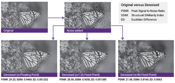
Figure 2. A 12-bit fixed-point implementation of the Denoiser algorithm delivers results practically indistinguishable from those of a floating-point implementation, while eight-bit fixed-point results exhibit more obvious lasting noise artifacts (courtesy Synopsys).
Area
Some SoCs prioritize silicon area ahead of either performance or power consumption. A designer of an application processor intended for consumer surveillance applications, for example, might have limited area available on the SoC, therefore striving to obtain highest-achievable performance at a given die "footprint". Selecting the most advanced, i.e., smallest, process node available is often the best way to minimize area. Moving from 28nm to 16nm, or from 16nm to 12nm or lower, can both increase clock frequency capabilities, reduce power consumption at a given clock speed, and decrease die size. However, process node selection is often dictated by company initiatives that are beyond the SoC designer's influence.
Selecting an optimized embedded vision processor is the next best way to minimize area, since such a processor will maximize the return on the silicon area investment. Another way to minimize area is to reduce the required memory sizes. For an EV6x core containing both a vision processor and a CNN "engine", for example, multiple memory arrays are present: for the scalar and vector DSPs as well as the CNN accelerator, along with a closely coupled partition for sharing data between the processing units. While memory size recommendations exist, the final choice is left to the SoC designer. Keep in mind, however, that reducing memory capacities could negatively impact system performance, among other ways by increasing bandwidth on the AXI bus. Another way to address memory size on the EV6x is to choose a single- versus dual-MAC configuration. Again, smaller area has to be balanced against higher performance.
Power Consumption
Consumer and mobile designers often list power consumption as the most critical constraint. A designer of an SoC for a mobile device, for example, might strive for the best performance within a 200 mW power budget. Fortunately, embedded vision processors are designed with low power in mind. Fine-tuning clock frequencies is the most straightforward way to lower the power consumption budget. A system that could perform at clock speeds as high as 1280 MHz might instead be clocked at 500 MHz or lower, at least in some operating modes, to optimize battery life and reduce heat dissipation. Doing so, of course, can degrade performance. Power consumption is affected by both area (e.g., transistor count) and frequency. Generally, the smaller the area and lower the transistor toggle rate, the less power your design will consume.
Bandwidth
Bandwidth on the AXI or equivalent interconnect bus is often a top concern, related to power consumption. Reducing the number of external bus transactions will save power. Increasing the amount of memory (at the tradeoff of higher required silicon area, as previously discussed) to decrease the number of required external bus accesses is one approach to actualizing this aspiration. However, deep learning research is also coming up with various pruning and compression techniques that reduce the number and type of computations, along with the amount of memory, needed to implement a given CNN graph.
Take a VGG16 graph, for example. Reducing the number of coefficients, through a pruning process that deletes coefficients close to zero and retrains the system to retain accuracy, can significantly reduce the number of coefficients that have to be stored in memory, therefore cutting down bandwidth. However, this process doesn’t necessarily lower the calculation load, therefore power consumption, unless (as with the EV6x) hardware support also exists to discard MAC operations with zero inputs. Using eight-bit coefficients when 12-bit support isn’t needed for accuracy will also lower both bus bandwidth and external memory requirements. The EV6x, for example, supports eight-bit as well as 12-bit coefficients and feature map values.
Gordon Cooper
Product Marketing Manager for Embedded Vision Processors, Synopsys
Software Optimization
While it's highly beneficial to fully leverage all available processing resources in a SoC and/or system, as discussed in the previous section of this article, it's equally important to optimize the deep learning-based vision software that's running on those processing resources. The following essay from BDTI explores this topic in detail, including implementation suggestions.
Optimization of a compute-intensive workload can be described in terms of one or multiple of the following levels of abstraction:
- Algorithm optimization: modify the algorithm to do less computation, and/or better fit the target hardware.
- Software architecture optimization: come up with a software architecture that maximizes system throughput, e.g., avoiding needless data copies, making efficient use of caches, enabling efficient use of parallel resources, etc.
- Hot-spot optimization: individually optimize the most time-consuming functions.
The greatest gains are often found at the highest levels of abstraction, and therefore highest-level optimizations should be undertaken first. A fully customized implementation of an application, one that has been thoroughly optimized at each of these levels and for the specific use case, will likely yield the best power/performance result. But such a time consuming and expensive development path may not be practical. For DNN deployment in particular, a full-custom implementation of a CNN is a risky undertaking: network topologies are evolving rapidly, and if you spend several man-months optimizing for one topology, by the time you’re finished you might find out that you should be using some other topology instead. Because of this risk, it's rare to see DNNs optimized to the last clock cycle or the last mW.
What's typically seen in practice, instead, are frameworks for deployment that don’t assume a specific topology. In terms of software architecture, these frameworks are designed to handle well-known published topologies such as ResNet50, GoogLeNet, and SqueezeNet. The underlying individual functions are also highly optimized, using these same well-known networks as benchmarks. Because these frameworks need to have a lot of flexibility, they can’t necessarily match the peak performance of a fully customized implementation.
Keep in mind, too, that that if you're striving to deploy a network that’s vastly different from the “benchmark” networks for which the framework was designed, you might end up with sub-optimal performance. A character recognition network that operates on 40×40 pixel images, for example, probably has a much smaller memory footprint than that found with commonly-used image classification networks, making the character recognition network amenable to optimizations that conversely wouldn't be effective in a framework designed to deploy larger networks (see sidebar "Optimization at the System Level, An Object Recognition Case Study").
Some examples of hardware vendor-provided frameworks for efficient deployment of DNNs include (not intended to be a comprehensive list):
- Intel’s Deep Learning Deployment Toolkit
- Nvidia’s TensorRT
- Qualcomm’s Snapdragon Neural Processing Engine
These particular DNN deployment frameworks are based on underlying libraries that are thoroughly optimized by the hardware vendor. In leveraging them, developers often have two implementation options:
- Use the deployment framework at a high level (i.e., simply feed it the network description and weights, and let automated tools do all the work), or
- In some cases it’s possible to make direct calls to the framework's underlying library API, thereby obtaining better results via some manual optimization of the implementation architecture.
Because the underlying library is so well optimized by the hardware vendor, both of these options can end up delivering better performance than what a developer could practically achieve otherwise, given limited budget and schedule, even though, as previously noted, a full-custom implementation would theoretically yield even better results.
One other note: since the deployment frameworks provided by hardware vendors need to be flexible enough to support various topologies, they often leave the first level of optimization listed at the beginning of this essay, algorithm optimization, to the developer. If you can design and train a smaller topology (measured by some combination of fewer weights, fewer activations, and/or fewer operations), you’ll likely end up with better performance. This may be the case even if your tailored implementation is seemingly less optimal because your resultant network now doesn't look like one of the well-known topologies for which the framework was initially designed.
Therefore, if you’ve selected a well-known topology that your research suggested would give you the smallest/fastest/etc. outcomes for your application, trained it, and ended up with acceptable results, ask yourself the following question: is the accuracy of your trained network limited by the topology design, or by the training methods (choice of optimizer, meta parameters), or by limitations of the training data, or by fundamental limitations of the application? It’s possible that you could shrink feature maps, remove layers, or tweak the network topology in various other ways to make the network smaller without losing much (if any) accuracy.
Conclusion
Vision technology is enabling a wide range of products that are more intelligent and responsive than before, and thus more valuable to users. Vision processing can add valuable capabilities to existing products, and can provide significant new markets for hardware, software and semiconductor suppliers. Deep learning-based vision processing is an increasingly popular and robust alternative to classical computer vision algorithms, but it tends to be comparatively resource-intensive, which is particularly problematic for resource-constrained embedded system designs. However, by making effective leverage of all available heterogeneous computing nodes, efficiently utilizing memory and interconnect bandwidth (both between various processors and their local and shared memory), and harnessing leading-edge software tools and techniques, it's possible to develop a deep learning-based embedded vision design that achieves necessary accuracy and inference speed levels while still meeting size, weight, cost, power consumption and other requirements.
By Brian Dipert
Editor-in-Chief, Embedded Vision Alliance
Senior Analyst, BDTI
Sidebar: Additional Developer Assistance
The Embedded Vision Alliance, a worldwide organization of technology developers and providers, is working to empower product creators to transform the potential of vision processing into reality. Au-Zone Technologies, BDTI and Synopsys, the co-authors of this article, are members of the Embedded Vision Alliance. The Embedded Vision Alliance's mission is to provide product creators with practical education, information and insights to help them incorporate vision capabilities into new and existing products. To execute this mission, the Embedded Vision Alliance maintains a website providing tutorial articles, videos, code downloads and a discussion forum staffed by technology experts. Registered website users can also receive the Embedded Vision Alliance’s twice-monthly email newsletter, Embedded Vision Insights, among other benefits.
The Embedded Vision Alliance’s annual technical conference and trade show, the Embedded Vision Summit, is coming up May 22-24, 2018 in Santa Clara, California. Intended for product creators interested in incorporating visual intelligence into electronic systems and software, the Embedded Vision Summit provides how-to presentations, inspiring keynote talks, demonstrations, and opportunities to interact with technical experts from Embedded Vision Alliance member companies. The Embedded Vision Summit is intended to inspire attendees' imaginations about the potential applications for practical computer vision technology through exciting presentations and demonstrations, to offer practical know-how for attendees to help them incorporate vision capabilities into their hardware and software products, and to provide opportunities for attendees to meet and talk with leading vision technology companies and learn about their offerings. More information, along with online registration, is now available.
The Embedded Vision Alliance also offers a free online training facility for vision-based product creators: the Embedded Vision Academy. This area of the Embedded Vision Alliance website provides in-depth technical training and other resources to help product creators integrate visual intelligence into next-generation software and systems. Course material in the Embedded Vision Academy spans a wide range of vision-related subjects, from basic vision algorithms to image pre-processing, image sensor interfaces, and software development techniques and tools such as OpenCL, OpenVX and OpenCV, along with Caffe, TensorFlow and other deep learning frameworks. Access is free to all through a simple registration process.
The Embedded Vision Alliance and its member companies periodically deliver webinars on a variety of technical topics, including various deep learning subjects. Access to on-demand archive webinars, along with information about upcoming live webinars, is available on the Alliance website. Also, the Embedded Vision Alliance is offering offering "Deep Learning for Computer Vision with TensorFlow," a series of both one- and three-day technical training class planned for a variety of both U.S. and international locations. See the Alliance website for additional information and online registration.
Sidebar: Optimization at the System Level, An ADAS Case Study
The design project discussed in the following case study from Au-Zone Technologies, developed in partnership with fellow Alliance member company NXP Semiconductors, showcases real-life implementations of the heterogeneous computing and software optimization concepts covered in the main article, along with other system-level fine-tuning optimization techniques.
As with any computer vision design exercise, system-level optimization must be taken into consideration when creating deep learning-based vision processing solutions. Considering the raw volume of data created by a real-time video stream, the compute horsepower required for real-time CNN processing of the stream, and the limitations imposed by embedded SoCs, optimization at every opportunity during development and deployment is essential to creating commercially practical solutions.
To make these system-level design optimization concepts more tangible, this case study describes the development of a practical TSR (traffic sign recognition) solution for deployment on NXP Semiconductor’s i.MX8 processors. In this example, we focus on the principal areas of system optimization within the constraints imposed by a typical embedded system:
- Deploying a deep learning-based vision processing pipeline on a heterogeneous platform
- Neural network design choices and tradeoffs
- Inference engine performance optimizations
Although this case study focuses on a specific image classification problem and processor architecture, the design methodology and optimization principles can be generalized to solve many different embedded vision processing and classification problems, on divergent hardware.
System Design Objectives and Optimization Approaches
Using as little compute horsepower as possible, the overall objective of this project was to design a practical object detection and classification solution characterized by the following boundary conditions:
- Robust TSR detection and classification using only standard optics, sensors and processor(s)
- Real-time processing of the video stream coming from a camera
- Classification accuracy greater than 98% on test data, and greater than 90% on live video
- Low-light performance suitable for automotive market applications
- A cabling solution able to provide 2-3m separation between the camera head and compute engine
- The use of automotive-grade silicon (sensor, processor and supporting components)
- The use of best-in-class computer vision techniques to implement the vision pipeline
- An overall system cost that is appropriate for the market application
Focusing on an overall system optimization forces the developer to consider many different, often conflicting, design and performance aspects to find a balance that is appropriate for a given application. The following diagram highlights some of most common parameters that need to be considered in any development program (Figure A). Depending on the application, market and performance objectives, the relative priority of these parameters will vary.
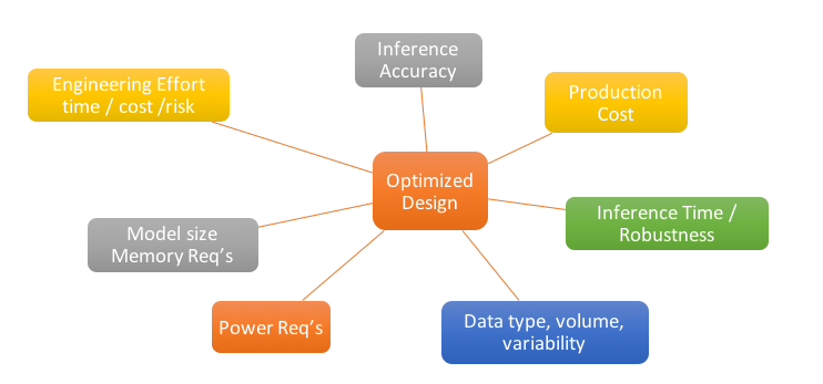
Figure A. The relative priority of various common system design optimization parameters will vary depending on the particular application and other variables (courtesy Au-Zone Technologies).
Taking a holistic approach to maximize accuracy while minimizing compute cost (time and energy), production hardware cost (engineering bill of materials, e.g., eBOM) and engineering effort often becomes a challenging balancing act for designers. System design for a deep learning-based vision solution is an iterative process; you will need both a starting point and a general framework on how to approach the problem in order to deliver a commercially viable solution within a resource constrained design.
Although there is no single recipe to follow, the following outlined sequence provides a generalized framework for your consideration. Assuming the objective for your project will be to implement a real-time classification system with optimum accuracy on lowest-cost hardware, the developer should consider optimization in the following order of diminishing returns:
- Minimize data volume and processing requirements
- Distributed processing, pipelines, and heterogeneous computing
- Optimization of individual vision pipeline stages
- Image Processing
- Object Detection
- Object Classification
Minimize Data Volume and Processing Requirements
It may seem obvious, but an easy trap to fall into when designing an embedded imaging system involves using commonly available cameras and image sensors, which are designed to provide extremely high image quality. The development team architecting the hardware may identify sensors that are convenient from a hardware design perspective, for example, without having visibility into how this decision may make the downstream processing problem overly complex or even impossible to solve on a given platform. Often, such devices produce data streams with image quality and resolution far exceeding what is actually required to solve common recognition or classification problems, making all subsequent processing steps much more complicated than necessary.
Specific image sensor (and camera) parameters affecting the data rate include:
- Color vs monochromatic capture
- Pixel depth
- Frame rate
- Image resolution (i.e., what is the minimum viable resolution necessary to solve the problem?)
- Scaling (nearest-neighbor or interpolation)
- Binning (2×2, 4×4 grouping)
- Data type/format/color space (e.g., RAW, Bayer, YUV, RGB, etc. (Figure B))
Pursuing all opportunities to minimize data input and reduce complexity at the front end will provide significant benefits downstream.
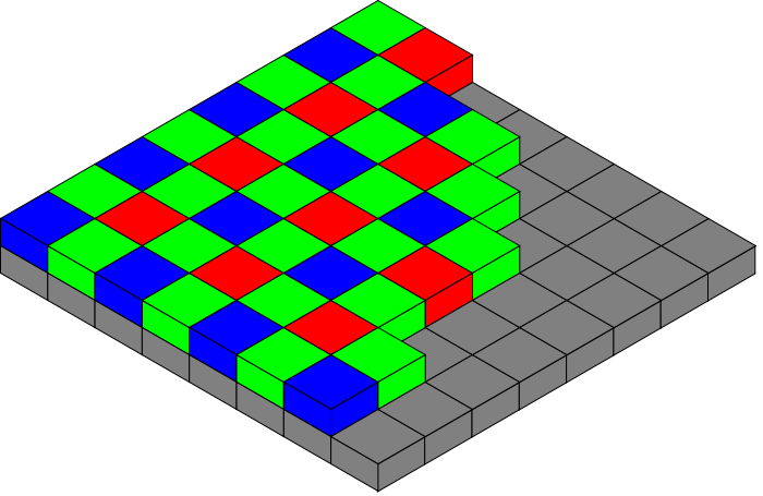
Figure B. The output format and other characteristics of the image sensor, such as in this Bayer filter pattern approach, can greatly affect the payload size of the data stream to be subsequently processed (courtesy Au-Zone Technologies).
Distributed Processing, Pipelines, and Heterogeneous Computing
The Wikipedia definition for heterogeneous computing refers to "systems that use more than one kind of processor or cores. These systems gain performance or energy efficiency not just by adding the same type of processors, but by adding dissimilar coprocessors, usually incorporating specialized processing capabilities to handle particular tasks."
Given the overall computational load required by a deep learning-based vision solution running at a robust frame rate, the first significant design optimization opportunity is to map the vision pipeline to a heterogeneous compute platform with processing elements that are well suited to each stage in the pipeline. The following diagrams show the simplified mapping between our TSR pipeline and the corresponding hardware compute elements in the i.MX8 based system (Figure C).


Figure C. A simplified visualization of the vision processing pipeline used to implement this project (top), can be mapped onto various heterogeneous processing elements in the target SoC (bottom) (courtesy Au-Zone Technologies).
Optimization of Individual Vision Pipeline Stages
One consequence of this pipelined computing architecture is a derived system design optimization constraint for the entire pipeline: to ensure that the data type and format of the processed data from one stage maps well to the next. Unnecessary data movement or format conversions between any stages will result in needless compute time and energy consumption.
It’s worth noting that implementing the ‘fastest’ solution at each stage in the pipeline, and/or the fewest total number of stages to construct the pipeline, will still not always result in a fully optimized solution if translations are still required. For this reason, it becomes very important to evaluate overall end-to-end performance of the system before ‘committing’ to any specific element in the vision pipeline or supporting hardware. In this case study, the two highest-cost processing functions in the vision pipeline are detection (since the entire scene must be processed) and classification (due to the high compute requirements for the CNN). Focusing on first minimizing these two stages results, at least in this case, in the best end-to-end efficiency.
The image sensor selected for the case study is one concrete example of this kind of design optimization. In order to provide good low light performance for automotive applications, we selected a high dynamic range image sensor which also includes a basic on-chip ISP (image signal processor) block, whose image quality optimization capabilities (de-Bayering, white balance, auto exposure and aperture/gamma corrections) offloads later pipeline stages from needing to accomplish these tasks. However, this image sensor only has two output color format options, YUV and RAW, which imposes a color space constraint on the following stages.
In other cases, therefore, the designer may decide to use an image sensor with support for other color space output options, alternatively perform ISP functions downstream, or design a system with no ISP in order to optimize for bill-of-materials cost. Designing a deep learning system with no ISP suggests the need for a custom training dataset that has generated using a similar imaging pipeline, thereby shifting cost from hardware to the front end development effort. This tradeoff may be favorable if a custom dataset is required, anyway.
Color Space Conversion
Since detection and classification are the two most expensive system functions in the pipeline, finding the most efficient method to implement each of them, along with providing each of them with an optimum input format, is crucial to developing an efficient solution. The principle objective of the color space conversion stage is to transform the input frames coming from the image sensor into formats well suited for each of these stages. The following diagram summarizes this process (Figure D). The ordering of the conversion sequence may seem odd at first glance, with YUV→RGB conversion first, followed later by the classification stage. However, this ordering is beneficial: the overall YUV→RGB→GRY (greyscale) conversion implementation cost ends up being lower than would be the case using other approaches.
Figure D. The particular color space conversion sequence used in this project was selected in order to minimize the total implementation cost (courtesy Au-Zone Technologies).
Since the GTSRB (German Traffic Sign Recognition Benchmark) training images, for example, are RGB in format, as are the images operated on by most deep learning CNNs, this format is required for the classification stage. The lowest-cost method to convert from YUV to RGB makes use of a well-known technique described formulaically as:
R = 1.164(Y – 16) + 1.596(V – 128)
G = 1.164(Y – 16) – 0.813(V – 128) – 0.391(U – 128)
B = 1.164(Y – 16) + 2.018(U – 128)
The pipeline sequence buffers this image format for subsequent processing in the classification stage, after performing detection and identifying regions of interest.
Object Detection
Since the detection stage must process all pixels in the field of view in order to identify high-probability candidate opportunities to subsequently classify, the detection stage must be very efficient. Although implementing a CNN-based detector is possible, traditional computer vision-based detection techniques are often much more computationally efficient. These computer vision operations can also often be performed in greyscale format without loss in accuracy, thereby providing a 3:1 reduction in pixel processing at the cost of upfront conversion. The format conversion from RGB to greyscale is described formulaically as:
GRY = (R * 0.2126 + G * 0.7152 + B * 0.0722)
Due to the highly parallel nature of both of these color space conversions, they can be accomplished very efficiently, and at full resolution and frame rate, by shader kernels running on the GPU. The overall cost of these conversions is insignificant in terms of the overall end-to-end processing time, and they make the two critical stages very effective.
The candidate detection algorithm scans every frame to look for high probability regions of interest where traffic signs are likely to be present. It is a first-order search, only performing detection without any attempt to classify. Using traditional computer vision techniques, the algorithm detects the basic shapes of traffic signs (such as circles, triangles, and rectangles) in the overall scene and generates a corresponding ROI (region of interest). This is done by first extracting the edges in the image with a Sobel filter then processing those edges for contours.
Once regions of interest are determined by the detection stage, the corresponding ROI parameters are then passed to the CNN stage of the pipeline for classification. The overriding goal of the detection stage is high recall, i.e., false positives are acceptable as long as false negatives (missed detections) are minimized. This tradeoff ensures that all reasonable candidates will pass to the CNN stage for classification; the CNN will handle rejections as part of its subsequent processing.
Object Classification
With one or more high probability candidate regions identified in a scene, the specific pixel data from the RGB image for each ROI is passed to the CNN for classification. Any given scene may contain multiple candidates that require classification, which are therefore processed sequentially (Figure E). Since the distance to the object is variable, and since the input side of the neural network is fixed in resolution, the neural network candidate ROIs are first scaled to match the neural network input.
Figure E. Any given scene may contain multiple traffic sign recognition candidates requiring sequential classification (courtesy Au-Zone Technologies).
Optimizing inference involves the consideration of several factors. First and foremost is the tradeoff between execution time and accuracy; larger, more complex networks can sometimes provide higher accuracy, but only within limits. And when optimizing execution time, you should focus on two general areas: network design optimizations and runtime inference optimizations.
Network Design Optimizations
The most important aspect to consider when designing a neural network to solve a classification problem is to make sure that it is of an appropriate size and depth. Example networks can be plotted on a graph with respect to their accuracy versus compute time at various model sizes, and then grouped into three general categories based on the complexity of the image classification problem they are appropriate for solving (Figure F). One network type or size does not solve all problems, and perhaps even more importantly, larger networks are not always better if real-time performance is important for your application.
Figure F. A comparison of various network model options organizes them with respect to both their accuracy versus compute time at various model sizes, and the complexity of the image classification problems they're appropriate to solve (courtesy Au-Zone Technologies).
In examining the example networks in the medium complexity category in more detail, for example, you'll discover the multiple tradeoffs to be made within this subgroup (Table A). The relative priority of accuracy, inference time and memory usage in your design situation will be reflected in a particular ranking for the various examples.
|
Network Topology |
Input Resolution |
Layers / Weights |
Training Accuracy † |
Runtime (MB) |
Inference (msec) |
|
TSR Net |
24 x 24 |
8 / 500K |
97% |
2.0 |
1.4 |
|
TSR Net |
56 x 56 |
8 / 2.5M |
97% |
10.0 |
7.2 |
|
Fully Convolutional (FCN) |
24 x 24 |
5 / 275K |
95% |
0.5 |
1.0 |
|
Multi-Layer Perceptron (MLP) |
24 x 24 |
2 / 1M |
78% |
1.5 |
0.8 |
|
ResNet * |
24 x 24 |
18 / 260K |
97% |
1.2 |
8.5 |
|
SqueezeNet * |
24 x 24 |
12+ / 5M+ |
98% |
5 |
5.0 |
Table A. A comparison of medium-complexity neural networks implemented on a desktop computer (notes: †=inference accuracy after 100 epochs of training, *=custom network designs with key features derived from named network) (courtesy Au-Zone Technologies)
Key takeaways from this data include the fact that the use of higher resolution inputs for training, testing and/or live video does not demonstrably improve accuracy, but will have a significant negative impact on runtime size and inference time. To be specific, further testing based on desktop computer evaluation showed that the 24 x 24 input resolution setting was optimal. Also, slightly reducing the accuracy expectation (-2%) compared to a fully convolutional network enabled reducing inference time by more than 6 ms.
With the TSRnet topology, for example, calculating the distribution of compute time across the network layers enables a developer to quickly focus on layers that are consuming the most compute time, targeting them for further optimization (Figure G). If bottlenecks become apparent with a given network model, the developer can modify the network to simplify or eliminate layers, subsequently retraining and retesting quickly.
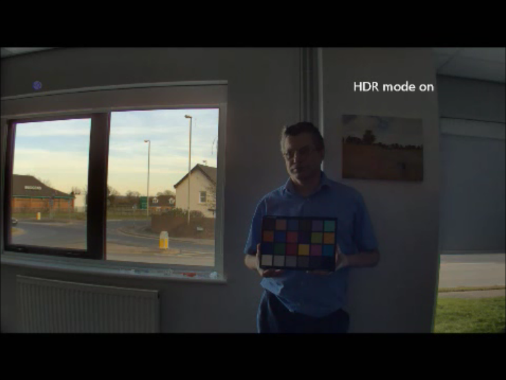
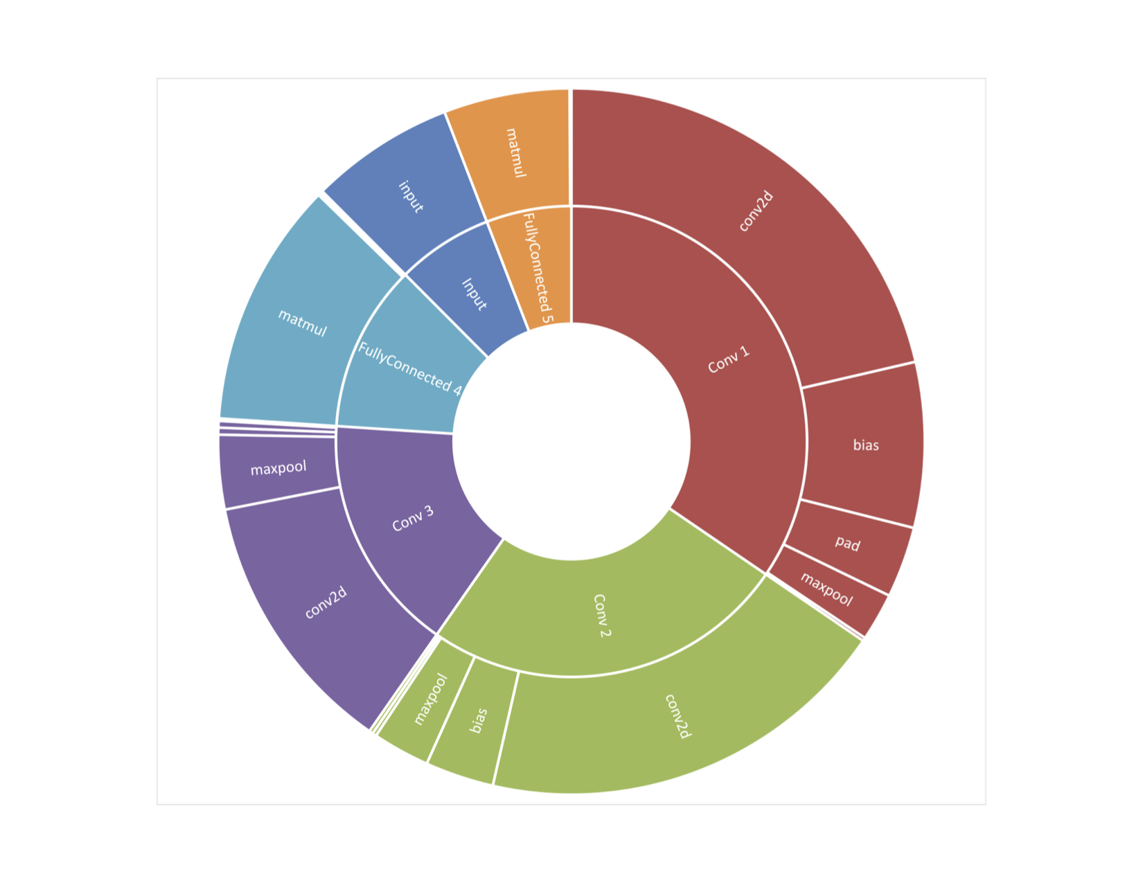
Figure G. With the TSRnet topology (top), calculating the distribution of compute time across the network layers rapidly identifies layers consuming the most compute time (middle), which are targets for further optimization (bottom) (courtesy Au-Zone Technologies)
Runtime Inference Optimizations
With a suitable neural network design capable of solving the classification problem evaluated on a desktop computer to use as a starting point, the next obstacles to overcome are to implement that network on the resource-constrained embedded target, and then optimize the embedded implementation for efficiency. When implementing the runtime on the embedded target, the developer has several options, each with tradeoffs, to consider:
- Code the model directly using existing libraries such as ACL, BLAS, Eigen and processor-specific methods. This is a particularly good option if few network design iterations or processor-specific optimizations are required to reach an appropriate solution.
- Modify existing open-source training frameworks to perform inference on your embedded platform.
- Leverage TensorFlow Lite to retrain an existing model on your data. This is a particularly good option if the problem you’re working on fits well with existing network design and supported core operations. Also, this option straightforwardly targets Android and iOS platforms.
- Implement a dynamic inference engine capable of loading and evaluating models. This is the "long game" option, requiring the most upfront investment to achieve a fully optimized solution capable of loading and evaluating different network topologies. The benefit of this investment is an engine fully optimized for any particular processor architecture and fully independent of the network design.
For this case study, we pursued option 4, using the DeepViewRT Run Time Inference Engine to target execution of the neural network on the processor. Table B shows inference times evaluated on the i.MX8 processor, and using the DeepViewRT dynamic inference engine for the same networks previously described in Table A.
|
Network Topology |
Input Resolution |
Layers / Weights |
Training Accuracy † |
Runtime (MB) |
Inference (msec) |
|
TSR Net |
24 x 24 |
8 / 500K |
97% |
2.0 |
2.8 |
|
TSR Net |
56 x 56 |
8 / 2.5M |
97% |
10.0 |
14.0 |
|
Fully Convolutional (FCN) |
24 x 24 |
5 / 275K |
95% |
0.5 |
9.5 |
|
Multi-Layer Perceptron (MLP) |
24 x 24 |
2 / 1M |
78% |
1.5 |
2.5 |
|
ResNet * |
24 x 24 |
18 / 260K |
95% |
1.2 |
3.9 |
|
SqueezeNet * |
24 x 24 |
12+ / 5M+ |
<80% |
5 |
>1000 |
Table B. A comparison of medium-complexity neural networks implemented on the i.MX8 embedded target (notes: †=inference accuracy after 100 epochs of training, *=custom network designs with key features derived from named network) (courtesy Au-Zone Technologies)
Regardless of the particular path you choose to implement run-time inference, the overall objective remains the same: to minimize the system compute load and time required to perform inference for a given network on a particular target processor. Optimizations for resource-constrained embedded processors cluster into two general categories: compute techniques, and processor architecture exploits.
Compute Techniques
Compute techniques are generally portable from one hardware platform to another, although the benefits seen on one processor are not always duplicated exactly on another. Some specific areas of optimization to consider are outlined in the following lists.
Neural network and linear algebra libraries:
Computational transforms:
- The Toeplitz matrix
- Winograd
- Strassen
- Filter decomposition
Separable convolutions:
- Computational data format ordering: NHWC, NCHW, NCHW, etc…
- N refers to the number of images in a batch.
- H refers to the number of pixels in the vertical (height) dimension.
- W refers to the number of pixels in the horizontal (width) dimension.
- C refers to the channels. For example, 1 for black and white or grayscale and 3 for RGB.
Data I/O optimizations:
- Data reuse
- Dimensional ordering
- Image data reuse
- Filter data reuse
- Tiling: blocking vs linear
- Kernel and layer fusing
Processor Architecture Exploits
Hardware specific optimizations are typically processor architecture specific and are not assumed to be portable. Some specific examples are outlined in the following lists.
Processor core type and instruction set
- CPU
- GPU
- Vision DSP
- FPGA
- Neural network processor
Memory use optimization
- Registers
- L1 and L2 cache
- SRAM vs DRAM, and standard vs DDR (double data rate) memory interfaces
- Cache line/non-strided accesses
- Float, half, fixed data formats
- Bit width tradeoffs
- Non-linear quantization
Brad Scott
President, Au-Zone Technologies
Sidebar: Optimization at the System Level, An Object Recognition Case Study
In developing an optimized deep learning-based embedded vision design, putting realistic constraints on the characteristics of images (and kinds of objects in those images) that the classifier will be tasked with handling can be quite impactful in terms of reducing the required implementation resources. However, it's equally important to expand those constraints as needed to comprehend all possible image data scenarios. The following case study from BDTI, based on a real-life research project for a client, covers both of these points.
The goal of this project was to train a classifier that achieved very high accuracy (above 99%) on 25 object categories, while also being practical to implement on an embedded platform. The project was very exploratory in nature; the target hardware had not yet been defined, so we had no specific constraints on compute load, storage, or bandwidth. However, we could not assume that "cloud" connectivity was available; inference had to happen entirely in the embedded system.
We knew that we could make some reasonable assumptions about the data: the object of interest was always in a known region of the image, for example. The distance from the camera to the object of interest would also be measured separately from the image classifier, so that the classifier could assume that images were appropriately scaled and cropped using this information. These assumptions meant that the inputs to the classifier would be fairly uniform in position and scale, and we would therefore be able to design a “lightweight” classifier for the job.
In designing a classifier CNN based on these assumptions, we selected kernel sizes, feature map sizes, etc. to limit the compute load and memory footprint (including the number of weights and the size of activation matrices). In considering the effort to implement the CNN on an embedded CPU/DSP, we therefore also deliberately avoided normalization layers and other features that would have increased coding effort.
We were initially given both a training dataset and a validation dataset. At the end of the project, we would also receive additional test sets, which would include input conditions not covered in the training and validation datasets. By measuring accuracy on these test sets, we would be able to determine how well the initial training had generalized to the additional situations in the test sets. However, we were not allowed to see the test sets in advance, and we did not know what kinds of conditions would be present in the test sets. In general, this is non-ideal practice: a good rule of thumb is that artificial neural networks only learn what they are shown, and they can’t be expected to generalize to conditions not covered in training. Unfortunately in this case we didn’t even obtain any up-front information about the range of input conditions in the test sets.
The training and validation datasets consisted of images captured under uniform and otherwise optimum conditions: good visibility of the objects of interest, good lighting, etc. We were therefore able to rapidly design a lightweight CNN classifier and train it to achieve over 99.9% accuracy on the validation dataset. But we knew that the training and validation sets' conditions were too close to ideal, and it was therefore very unlikely that this initial training would generalize well to more diverse conditions. So we next used simple image processing techniques to simulate more challenging conditions such as occlusions, shadows, and other types of image noise.
We created a new validation set with these simulated challenges. On it, the network we had originally trained initially scored only 66.7% accuracy; not at all surprising, because it was not trained to deal with the simulated challenges. We then added these same simulated challenge conditions to the training set. We also created a custom layer in Caffe to on-the-fly simulate random occlusions during training. We retrained the network, which then achieved 100% accuracy on the original validation set, and 99.2% accuracy on the simulated-challenge validation set. And on the three test sets that we subsequently received, our network accuracy scores were as high as 99.9%.
We estimate that the CNN we designed could execute inference in a few hundred msec on a fully loaded 1 GHz NEON-supportive ARM core, and with no need for a GPU as a co-processor; a very lightweight and otherwise embedded-friendly design. Note that since this project focused only on initial network topology design and training, subsequent pruning or quantizing of the network was not explored, and memory "footprint" estimates are therefore not available. However, we believe that pruning and quantization (with retraining) would be very effective, with a negligible resultant reduction in accuracy.

